This thread has been locked.

If you have a related question, please click the "Ask a related question" button in the top right corner. The newly created question will be automatically linked to this question.

DP83869HM: MII Loopback failing, RX clock increasing in frequency during MII loopback

Part Number: DP83869HM
Other Parts Discussed in Thread: DP83869

We have a board for a new design but it does not pass MII loopback at 1G.  Some of the messages go through OK, but others contain errors.  In the error messages, we have observed the RX clock increasing from 125Mhz to approximately 140MHz.  In the messages that are OK, the RX clock stays at 125Mhz.  Any ideas on what could cause this?  Any suggestion on how to resolve?

We have ran the loopback software on both an earlier design board which used a DP83867 and on a different project's board that has a DP83869HM.  The loopback works with no errors on both of these.

Thanks,

Ron

  • Hello Ron, 

    Thank you for the reply.

    Not the ground pad, i was asking about the IC view where i see it as rectangular.

    Regards,

    Sreenivasa

  • I think it is the rotation angle of the 3D.  Does this help?

  • Hello Ron, 

    Thank you for the reply. 

    I think it is the rotation angle of the 3D.  Does this help? Yes this helps.

    Regards,

    Sreenivasa

  • Hello Sreenivasa,

      We were finally able to test with the load caps on other side of crystal.  The results seem to be the same, no better and no worse. 

      On a different PHY, we tried the cap divider on the FPGA 25Mhz output. For some reason, this PHY is now not recognized on the MII bus.  We will investigate as to why.  My guess is either there is a connection issue or the values of the caps is causing the input to be too low.

      On a third PHY, we tried the forcing it to master, but it remained as slave.  Will you help identify what we should be writing to the registers to force it to master mode?  Following is from our software engineer:

    Configured in MII loopback mode, I queries the GEN_STATUS1 (0xA) register for master/slave status at 10/100/1000.  In each case it reported as “Slave”.  I attempted to manually configure it as Master on the GEN1_CFG1 register (0x9), but the GEN_STATUS1 status register still reported as slave.  I’m not sure why the setting is not taking.  Perhaps we can ask TI if I need to do something different in my initialization sequence.  Here are the register read/writes I performed trying to configure PHY2 for loopback as master:

    Start PHY autonegotiation (Modified for DP83869HM - loopback max requested speed 1000)

    GEN_CTRL Register (0x001F) reporting 0x0000

    GEN_CTRL Register (0x001F) writing 0x8000

    BMCR Register (0x0000) reporting 0x1140

    BMCR Register (0x0000) writing 0x0140

    RGMII_CTRL Register (0x0032) writing 0x00D0

    BMCR Register (0x0000) reporting 0x0140

    BMCR Register (0x0000) writing 0x4140

    GEN_CFG1 Register (0x0009) reporting 0x0300

    GEN_CFG1 Register (0x0009) writing 0x1B00

    IO_MUX_CFG Register (0x0170) reporting 0x0C10

    IO_MUX_CFG Register (0x0170) writing 0x0C10

    IO_MUX_CFG Register (0x0170) reporting 0x0C10

    GEN_CTRL Register (0x001F) reporting 0x0000

    GEN_CTRL Register (0x001F) writing 0x4000

    GEN_STATUS1 Register (0x000A) reporting 0x0000

    MS_CONFIG_RES for phy address 7: Slave

    PHY_STATUS Register (0x0011) reporting 0xA802

    link mode for phy address 7: Full

    GEM 0xFF0D0000 configured for 1000

  • Hello Ron, 

    Good morning and thank you for the reply.

    I see that MII loopback has been configured in the registers shared. Configuring the register 0x16 should  configure the device as master.

    Could you please try configuring the PHY for any of the other loopbacks as below.

    Address 0x16 = 0x0004 or 0X0008

    Address 0x00 = 0x0140

    Address 0x1F = 0x4000

    Address 0x00FE = 0xE720

    Regarding the hardware changes, did you move the crystal position to the load cap position. Do you want to move the crystal nearer to the PHY and do a tests. Would it b possible to add a 100-200R series resistor at the Xi input.

    Regarding the FPGA clock - is the clock output 2.8V or 3.3V. The cap value changes with he voltage level.

    Is there any other signals that are passing near or close to the Xi. Ex: For 867 the MDC pin is next to the Xi pin. 

    Regards,

    Sreenivasa

  • Hi Sreenivasa,

    Thanks for the response.  We will try the suggested register values to see if we can force to master mode.  

    On FPGA driving XI, the clock output is 2.8V from the FPGA.  Our guys will be in the lab tomorrow to probe and see what the Xi signal looks like with the cap divider circuit.  Do you have a recommend value for the 2.8V output?  The word document Joe forwarded to us had 27pF for 3.3V, but not a recommend value for 2.8V.  Our plan was to analyze the signal to determine which value to try next.

    For the PHY with crystal providing Xi, we did not relocate the crystal, just moved the load caps.  Our plan is to install a pot in series to see the effect of different values.  With this, we can test the 100-200 ohms you suggested.

    I have asked our board layout engineer to identify any near by signals to Xi.  We looked at this early on, but did not identify any of concern.

    Thanks for your Support,

    Ron

  • Hello Ron, 

    Thank you for the reply.

    Please note that the cap divider was used with the DP83867 which had 1.8V or 2.5V or 3.3V IO and the clock range was always 1.8V.

    The DP83869 input scales with the VDDIO.  The below threads could help.

    https://e2e.ti.com/support/interface-group/interface/f/interface-forum/995787/dp83867ir-how-do-we-calculate-capacitor-value-when-we-use-2-5v-ocillator

    For 2.5V, recommended capacitor values are CD1=27pF and CD2=16pF. For 3.3V clock, capacitor values CD1=CD2=27pF is ok.

    Here is a post with explanations and derivations for the capacitor values:

    https://e2e.ti.com/support/interface-group/interface/f/interface-forum/805173/dp83867ir-xi-input-voltage-for-dp83867/2987238#2987238

    Checking with a POT is a good idea. The challenge could be the POT resistance resolution. A multi turn port has to be considered.

    When you are experimenting with the hardware, may be moving forward the crystal would be an option to consider.

    If possible could you shar the actual crystal part number. I can check with the design team here if they have any thoughts on the used crystal.

    Regard,

    Sreenivasa

  • Hi Sreenivasa,

      What is the "Address 0x00FE = 0xE720"?  Is that a type-o?  I cannot find that register.

    Thanks,

    Ron

  • Hello Ron, 

    Thank you for the message.

    Please refer below statement in the datasheet in section 9.3.4.1 Near-End Loopback

    When configuring loopback modes, the Loopback Configuration Register (LOOPCR), address 0x00FE, should be set to 0xE720.

    Regards,

    Sreenivasa

  • Hi Sreenivasa,

      Thanks for the response.  We were able to test on our PHY2.  We were able to put PHY2 into MASTER mode and verify.  As you advised, we had to use a different loopback mode instead of MII loopback.  The same loopback errors continued as before.  Does this imply a bad crystal source or a bad PLL or interference from another signal in layout?

    • The build with CLK_OUT = 25MHz Internal PHY Reference Clock (0xCXX) showed the Rx_CLK still increasing to >140MHz during bad messages but the CLK_OUT stayed at 25±0.2MHz. I can post o’scope capture if needed.
    • The build with CLK_OUT = Some Mystery 125MHz Clock (0xDXX, NOT in datasheet but believe to be a 125MHz reference clock from the PHY PLL) showed the Rx_CLK and CLK_OUT increasing to >140MHz and back to 125MHz together during bad messages. Captures available if needed.
  • Hi Sreenivasa,

     On PHY1, where we have the FPGA driving the XI input, we found a wiring error when cap divide was added.   We fixed and PHY1 is functional again, but with same errors.  Although the clock at XI is in the recommended operational range, the errors previously seen with the UDP tests were still seen (i.e. no auto-neg at 100MHz), which seems to go against the idea that the FPGA clock was overloading the Xi input and causing double clocking and/or misclocking.  We have scope captures and I can send if needed.  This was our work around path until we could find root cause on why the crystal oscillator was not working.  Should we try the loopback on this like we did using PHY2 (where crystal is driving XI)?  Any suggestions on how we can move forward?

    Thanks,

    Ron

  • Hello Ron, 

    Thank you for the update.

    Can you help me understand if you tried the digital and the analog loopback.

    The build with CLK_OUT = 25MHz Internal PHY Reference Clock (0xCXX) showed the Rx_CLK still increasing to >140MHz during bad messages but the CLK_OUT stayed at 25±0.2MHz.  

    Can you please confirm if this frequency change was observed during communication. 

    When you do not communicate, do you still see the frequency being stable.

    Can you please check if the TX_ER pin is routed close to Xi. Would it b possible to disable the TX_ER on the MAC side for testing. Are there any other RGMII signals running close to the oscillator ?

    Regards,

    Sreenivasa

  • Hello Ron, 

    Thank you for the message. 

    What is the crystal frequency you are measuring. Can you please check if the clock out of 25 MHz looks stable.

    When applying an external clock, if the reset is released before the clock is stable, there could be some performance issue.

    Please check Figure 4. Power-Up Timing and confirm that the reset is released 200ms after the clock is stable.

    Can you configure the clock out for 125MHz transmitter clock output and check. 

    Do you have internal facility to generate and receive packets to perform 0x8 = Reverse Loopback

    Regards,

    Sreenivasa

  • Hi Sreenivasa,

      Providing answers in blue to your questions:

    Can you help me understand if you tried the digital and the analog loopback.  He ran with digital loopback, he plans to run analog loopback later, but may be after first of the year.  This was on PHY2 where we still have a crystal driving Xi. We would still like to know does this imply a bad crystal source or a bad PLL or interference from another signal in layout?.  

    The build with CLK_OUT = 25MHz Internal PHY Reference Clock (0xCXX) showed the Rx_CLK still increasing to >140MHz during bad messages but the CLK_OUT stayed at 25±0.2MHz.  

    Can you please confirm if this frequency change was observed during communication.  This is only during communication when a bad transfer occurs.  We believe the frequency change is causing the bad transfer.  We will have 70-80% good communication and the frequency does not change.  When we are able to trigger on a bad transfer, we have observed the frequency change. I have tried to upload a capture, but the web site is not allowing it.

    When you do not communicate, do you still see the frequency being stable.  The frequency is stable when there is no communication occurring.  It is also stable during good communication..

    Can you please check if the TX_ER pin is routed close to Xi. Would it b possible to disable the TX_ER on the MAC side for testing. Are there any other RGMII signals running close to the oscillator ?  I am told this pin is not active during the communication.  I have requested a list of other traces nearby Xi, but may be after the first of year before I can provide.  Early on, these other traces were looked at closely and the activity on those traces occurred before the communication started

  • Hello Ron, 

    Thank you for the information.

    Let me review and comeback. 

    Did you have a chance to perform the tests with series resistor on Xi and X0. This is expected to help in the case where there is some interference around the oscillator circuit.

    Regards,

    Sreenivasa

  • Hi Sreenivasa,

    Providing answers in blue to your questions. This is in regard to our PHY1 where FPGA is providing clock to Xi:

    What is the crystal frequency you are measuring. Can you please check if the clock out of 25 MHz looks stable. Yes, it is stable and CLK_OUT is stable.  I cannot upload the file, but here is a snip from my screen:

    When applying an external clock, if the reset is released before the clock is stable, there could be some performance issue.

    Please check Figure 4. Power-Up Timing and confirm that the reset is released 200ms after the clock is stable.  We do not meet this requirement when driving with the FPGA, however, we command a reset via software after the FPGA clock is stable.  I had understood the software reset command does the same function as the hardware reset.  Is this true?  The guys in the lab did do a quick test where after the system was running, we had a 60 second delay before the software configured the PHY.  During this time, the reset pin was manually reset by shorting a wire.  From this test, we did not see a difference.  

    Can you configure the clock out for 125MHz transmitter clock output and check. We can, but not sure this was done yesterday.  I don't see it in the scope captures.  It may be after the first of the year before we can collect this.

    Do you have internal facility to generate and receive packets to perform 0x8 = Reverse Loopback  Please provide clarification on what is needed to run this test.  Can it be done with a PC connected to the board?  If so, what do we do on the PC to accomplish this?  The other option we would have is to bring over the 867 board.  Do you have any test software we can use to run this test?

    Thanks,

    Ron 

  • Hi Sreenivasa,

      In response to your question "Did you have a chance to perform the tests with series resistor on Xi and X0. This is expected to help in the case where there is some interference around the oscillator circuit.":

    Yes we did.  Here are the notes from Chad:

    With the pot at 0Ω the signal into Xi was captured and save as the R3 reference waveform on the oscilloscope (2.96Vpp, High at 2.5V, white waveform on captures).  With Xo and Xi monitored, the pot was rotated until Xi looked to match the preferred input range of Xi with VDDIO=1.8V (set to 1.7Vpp, 0.1-1.8V).  The pot was at 200Ω.  The function generator was disconnected from PHY0 which is needed for the test, but when the generator was reconnected to PHY0 the PHY3 Xo and Xi signals degraded significantly both in shape and amplitude (consistent with enabling/disabling the function generator’s output).  Moving the generator’s ground location and pushing the connections away from the PHY3 test area we were able to get the clocks on PHY3 to look clean again but the Xi amplitude was lower than before (Xo was same as before).  Again the pot was rotated until Xi looked to match the preferred input range of Xi with VDDIO=1.8V, this time the pot was at 25Ω.  PHY3 communicated over the management bus (crystal functional) but no data was received at the PC (1000 or 10MHz) with the switch inline.  The switch was removed and data was received at the PC with a direct connection but with poor validity rate (50%)

    In summary, the series resistor did not seem to make a difference,

    Ron 

  • Hey Sreenivasa,

      Question for you.  Should we see any activity on the following pins during the initialization or configuration stages of the PHY?

    CLK_OUT

    RX_CNTL (38)

    RX_CLK (32)

    RX_D0 (33)

    RX_D1 (34)

    RX_D2 (35)

    RX_D3 (36)

    TX_CNTL (37)

    TX_CLK (29)

    TX_D0 (28)

    TX_D1 (27)

    TX_D2 (26)

    TX_D3 (25)

    A yes/no answer is OK.   It could be we are seeing what happens during the programming of the SoC.  Or could be they are in Hi-Z and we are seeing crosstalk.  Whatever it is we have observed some activity and may need to dig into it some more, unless this is expected behavior from the PHY.

    Hope you are getting the Christmas/New Year's break we are getting.  Today is our last day until we return on Tuesday Jan 4th.  Hope you have a blessed time with with your family and friends.  We are really looing forward to it.

    Thanks,

    Ron

  • Hello Ron and Chad, 

    Thank you for the detailed inputs.

    Could you please confirm that the series resistor changed on the PHY that was running with the crystal ? We would want to add the series resistors to the XI and XO inputs of the PHY or at the output of the crystal. 

    With the pot at 0Ω the signal into Xi was captured and save as the R3 reference waveform on the oscilloscope (2.96Vpp, High at 2.5V, white waveform on captures).
    With Xo and Xi monitored, the pot was rotated until Xi looked to match the preferred input range of Xi with VDDIO=1.8V (set to 1.7Vpp, 0.1-1.8V). The pot was at 200Ω.
    The function generator was disconnected from PHY0 which is needed for the test, but when the generator was reconnected to PHY0 the PHY3 Xo and Xi signals degraded significantly both in shape and amplitude (consistent with enabling/disabling the function generator’s output).
    Moving the generator’s ground location and pushing the connections away from the PHY3 test area we were able to get the clocks on PHY3 to look clean again but the Xi amplitude was lower than before (Xo was same as before). Again the pot was rotated until Xi looked to match the preferred input range of Xi with VDDIO=1.8V, this time the pot was at 25Ω.
    PHY3 communicated over the management bus (crystal functional) but no data was received at the PC (1000 or 10MHz) with the switch inline.
    The switch was removed and data was received at the PC with a direct connection but with poor validity rate (50%)

    Regards,

    Sreenivasa

  • Hi Sreenivasa,

    Providing answers in blue to your questions. This is in regard to our PHY1 where FPGA is providing clock to Xi:

    What is the crystal frequency you are measuring. Can you please check if the clock out of 25 MHz looks stable. Yes, it is stable and CLK_OUT is stable.  I cannot upload the file, but here is a snip from my screen:

    Can i ask you to confirm if the clock frequency is within 50-100 PPM of 25MHz 

    When applying an external clock, if the reset is released before the clock is stable, there could be some performance issue.

    Please check Figure 4. Power-Up Timing and confirm that the reset is released 200ms after the clock is stable.  

    We do not meet this requirement when driving with the FPGA, however, we command a reset via software after the FPGA clock is stable.  I had understood the software reset command does the same function as the hardware reset.  Is this true?  The guys in the lab did do a quick test where after the system was running, we had a 60 second delay before the software configured the PHY.  During this time, the reset pin was manually reset by shorting a wire.  From this test, we did not see a difference.  

    Following the Two Supply Sequence Diagram, clocking and Power up timing (Figure 4. Power-Up Timing) are important requirements for the proper operation of the device.

    If the reset is active before the clock is stable, the only way to to make the device function normal is the Pin reset. I see a pin ENET1_RESET_N coming from the MAC.

    Recommended sequence is Figure 5. Reset Timing.

    Not sure if you had a chance to do similar measurements on the PHY with he crystal. This is something we would want to capture.

    Regards,

    Sreenivasa

  • Hello Ron, 

    Question for you.  Should we see any activity on the following pins during the initialization or configuration stages of the PHY?

    With the assumption the the device is out of reset and supplies are stable here are the states

    CLK_OUT - Will have the crystal output.

    Signals from PHY to MAC.

    I expect the clock to be present. Other signal activities are dependent on the signal from the copper interface.

    RX_CNTL (38)

    RX_CLK (32)

    RX_D0 (33)

    RX_D1 (34)

    RX_D2 (35)

    RX_D3 (36)

    Signals from MAC to PHY - May be the clock output would be available.

    TX_CNTL (37)

    TX_CLK (29)

    TX_D0 (28)

    TX_D1 (27)

    TX_D2 (26)

    TX_D3 (25)

    A yes/no answer is OK.   
    The signals have been classified with answers.

    Regards,

    Sreenivasa

  • Hello Ron, 

    The idea here is to check reverse loopback and see if the clock is affected. 

    Do you have a EVM and a launchpad to program the PHY, If we use another of the equipment, the register changed required to be done would take time.

    Regards,

    Sreenivasa

  • Hello Ron, 

    If we configure the reverse loopback, we could use the PRBS as below.

    9.3.5 BIST Configuration

    The device incorporates an internal PRBS Built-In Self Test (BIST) circuit to accommodate in-circuit testing or diagnostics.

    Regards,

    Sreenivasa

  • Hello Ron, 

    Thank you for the message.

    Hope you are getting the Christmas/New Year's break we are getting.  Today is our last day until we return on Tuesday Jan 4th. 

    Hope you have a blessed time with with your family and friends.  We are really looing forward to it.

    You all have a merry Christmas and happy new year.

    Regards,

    Sreenivasa 

  • Hello Ron, 

    For the PHY with crystal providing Xi, we did not relocate the crystal, just moved the load caps.  Our plan is to install a pot in series to see the effect of different values.  With this, we can test the 100-200 ohms you suggested.

    I have asked our board layout engineer to identify any near by signals to Xi.  We looked at this early on, but did not identify any of concern.

    I assume you soldered wires to connect the function generator. The separate wires plus the drive capability of the function generator could be helping.

    Also i assume the function generator was on before the PHY is powered on. This would man the clock is stable before the reset is released.

    Regards,

    Sreenivasa

  • Hello Sreenivasa and Happy New Year,

      We have not been able to locate a EVM yet, will you provide a part number?  I sent Joe an email this morning, asking for the same info.  Also, what is a "launchpad"?  Is that just software or also hardware?  I will need a part number for that also.

      We are making a modification to allow the FPGA to control the PHY reset when the FPGA provides the clock, we plan on testing that later today.  Will let you know the results when complete.

    Thanks,

    Ron

  • Hello Ron, 

    Wishing you  a happy new year 2022.

    Thank you for the reply and updating the plan. Joe did follow-up on the same.

    Please refer below. One is the EVM

    https://www.ti.com/tool/DP83869EVM

    The launchpad is the programmer for accessing the MDIO registers on customer board if the MDIO interface is accessible. 

    https://www.ti.com/tool/MSP-EXP430F5529LP

    Regards,

    Sreenivasa

  • Hi Sreenivasa,

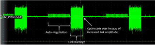
      We have ordered the EVM and programmer, still waiting for it to arrive.  In meantime, we are continuing to troubleshoot with O’scope.  We have added a reset line from the FPGA to hold the PHY in reset until the clock out of the FPGA is stable.  It now meets the timing per the datasheet, but still the PHY does not work at 1G when the FPGA provides the XI input, but does work when a function generator is used.  We have tried the with and without the cap divider, still does not work when using the FPGA.  When using the FPGA to provide XI, we thought it was not completing auto-negotiation, but looking closer it appears auto-negotiation is completing, but the link is not coming up. We expected to see an increase of amplitude but instead, it performs another auto-negotiation.  Following is from pins 1/2 on PHY with FPGA on XI:


    For comparison, following is when function generator is used for XI, we see an increase in amplitude as the link starts working:


    Any thoughts on what could be causing this?

    Thanks,

    Ron

  • To clarify, pins 1 and 2 are on the RJ-45 connector and we are using an active probe.

  • Hello Ron, 

    Thank you for the inputs.

    Couple of quick questions

    Is the same scale used for both the waveforms. The link pulse amplitudes do not mach.

    What is the link partner ( other device) used. Can you please compare the clock of both the boards.

    Can you Please compare the function generator waveform and the FPGA waveform shape and frequency?

    Instead of using a capacitor divider for the FPGA clock division, please consider using a resistor divider for testing purpose.

    Regards,

    Sreenivasa

  • Hello Sreenivasa,

    I am attempting to upload a file again, it would not work the other day.

    FPGA clock vs Function Gen

    This is a comparison of the Function Generator on PHY0  to the FPGA on PHY1.  Both are into the XI pin on PHYs.   One of the last things we did was to rewire PHY1 to use the function generator on XI.  This confirms both PHY0 and PHY1 work with the function generator providing XI input. 

    The amplitude differences may be due to me doing a snip of my screen then uploading.  I will see if I can now upload the files, earlier the system would not let me.

    Ron

  • Hello Ron, 

    On the FPGA generated clock i am seeing a step. Not sure if this is due to the FPGA port output type or the cap divider.

    Is there a way to check this.

    May be we could try an RC to remove the glitch.

    The Clock specs has impact on the MDI interface.

    Do you have a 25MHz oscillator in hand ?

    Regards,

    Sreenivasa

  • Hello Ron, 

    Can you please provide some inputs on these waveforms. I assume these are with the clock generated by the FPGA.

    PHY0 working

    PHY 1 not working

    Regards,
    Sreenivasa
  • The two waveforms are measured on RJ45 connector showing auto-negotiation on two different PHYs.  PHY0 completes and starts working, which is the top waveform.  The bottom waveform is PHY1 which completes auto-negotiation, looses the link and starts another auto-negotiation.

  • Hi Sreenivasa,

    Answers to your questions above:

    Is the same scale used for both the waveforms. The link pulse amplitudes do not mach.  No.  That is why I provided the two extra waveforms, which are at same scale.

    What is the link partner ( other device) used. Can you please compare the clock of both the boards.  This would be the Cisco switch.  And so no, cant compare clocks without disassembling the switch.  Doesn’t seem valuable since we see the switch port work fine with our other PHYs and with the same PHY but with the function gen clock.

    Can you Please compare the function generator waveform and the FPGA waveform shape and frequency?  Provided above

    Instead of using a capacitor divider for the FPGA clock division, please consider using a resistor divider for testing purpose.  Sure, we will add to our list to try.

    On the FPGA generated clock i am seeing a step. Not sure if this is due to the FPGA port output type or the cap divider.

    Is there a way to check this.  Capture of the pre & post cap divider clocks:

    May be we could try an RC to remove the glitch.  When you state glitch, is that the overshoot?

    The Clock specs has impact on the MDI interface.

    Do you have a 25MHz oscillator in hand ?   We don't have one on the shelf. We found one on a board we are going to attempt to salvage, not sure if it works or not. 

    Regards,

    Ron

  • Hello Ron, 

    Thank you for the below plot. The waveform looks fine but the amplitude looks less. We would need a 1.7V clock.

    Approach one is to adjust the cap to get the required amplitude.

    Second approach is to use a resistor divider to divide the 3.3V.

    The change in amplitude hopefully should resolve.

    Is there a way to check this.  Capture of the pre & post cap divider clocks:

    May be we could try an RC to remove the glitch.  When you state glitch, is that the overshoot?

    The Clock specs has impact on the MDI interface.

    Do you have a 25MHz oscillator in hand ?   We don't have one on the shelf. We found one on a board we are going to attempt to salvage, not sure if it works or not. 

    Regards,

    Sreenivasa

  • Hello Sreenivasa,

      We were able to get the clock from the FPGA to look better than the clock from the function generator, but it is still not working when using the FPGA as the input to XI.  Following is FPGA provided clock into XI and the CLK_OUT on PHY.


    Question, should the PHY work if the XI input is not active when power is applied, but is active before reset is released?

    Thanks,

    Ron

  • Hello Ron, 

    Thank you for the waveforms. I had an internal sync with the design team. The waveform looks fine.

    Would you be able to perform clock quality analysis (Jitter, Phase Nosie ) for the Xi input clock and the clock output. Please perform the same for both the clock output from the FPGA and the function generator.

    Regards,

    Sreenivasa

  • Hello Ron, 

    Could you please confirm if the waveform is with the cap divider or resistor divider. 

    The DP83867 has input range of 1.8V and hence capacitor divider was recommended.

    Optimization was done on the 869 to resolve this issue. 

    I am not sure if the performance would be optimal with the cap drop. SInce one of the concern is the signal quality, could you please replace the cap divider with equivalent resistor divider. Hopefully this should improve the performance.

    Regards,

    Sreenivasa

  • Hello Ron, 

    Question, should the PHY work if the XI input is not active when power is applied, but is active before reset is released?

    If the hardware reset is held low till the clock is stable, it is expected that the device should work.

    For testing, can you please toggle the Reset pin - Low to High, High to Low and Low to High (few us difference)

    Is there a way you could power up the PHY after the clock is available - again for testing.

    Regards,

    Sreenivasa


  • Hello Ron, 

    Please let me know if you can access the thread.

    Regards,

    Sreenivasa

  • Hi Sreenivasa,

      Yes, I can post again.

      Regarding holding the reset until the clock is stable, we did a quick test of disabling the function generator output while power was applied until just before the reset was released and the PHY worked, so we don't believe not having a clock when power is applied is the issue.

      Regarding your suggestion of "Would you be able to perform clock quality analysis (Jitter, Phase Nosie ) for the Xi input clock and the clock output. Please perform the same for both the clock output from the FPGA and the function generator.".  Unfortunately the signal analyzer we have in the lab  (Agilent N9010A EXA X-Series) does not have the phase noise package installed, but was able to get a bit of data anyways.  Both sources are extremely similar, no visible jitter or phase modulation in the traces.  The biggest obvious difference between the two clocks is that the SOC clock is stably running at 24.9567MHz while the function generator is stably running at 25.0000MHz.  This could be our issue. 

    We still don’t understand why it does not work with the crystal as originally designed. 

  • Hello Ron, 

    Thank you for the inputs.

    The PHY would tolerate around 100 PPM variation in frequency. the tolerance looks something around 1700 PPM.

    Regarding making it work with the on bard crystal, i will have to go through the thread on trails done. One of the discussion we were having was adding the series resistor and influence of adjacent signals on the clock.

    One way to test this would be to source an oscillator (similar to what we have on the EVM) and  wire it nearer to the oscillator.

    Did you receive the EVM by chance. We could tap the clock output from the oscillator to do a quick test.

    Regards,

    Sreenivasa

  • Hi Sreenivasa,

      I agree with you on the variation in frequency, we are looking to see if we can correct.

      We are still waiting on the EVM to arrive.  We have also order an oscillator, the one we had available was at the wrong voltage.

    Ron

  • Hello Ron, 

    Thank you for updating the status.

    Regards,

    Sreenivasa

  • Hello Ron, 

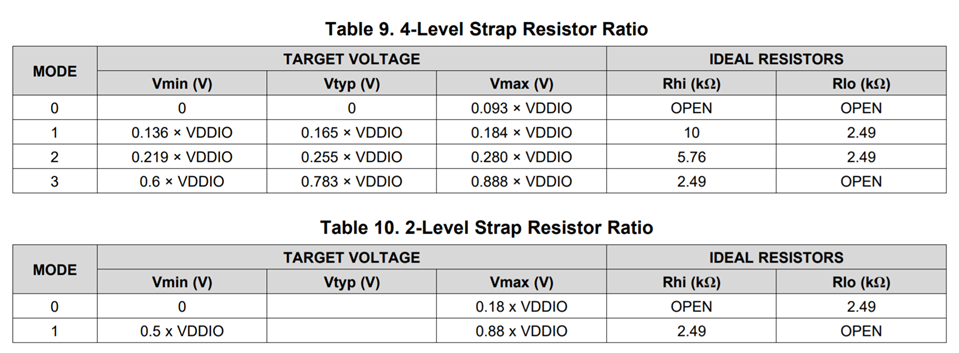
    One of the question during the call was on the strap values.

    Please refer below for the resistor ratios and the target voltages. These values are required  to be met for reliable reliably latching the straps. We have internally tested he performance for the recommended values.

    Regards,

    Sreenivasa

  • Sreenivasa,

      Thanks for the info.  Let me ask the question slightly different.  The datasheet states that the LEDs can be driven directly from the 3 LEDx pins but does not specify drive strength capability.  We are not driving the LEDs directly but would like to know that we did not stress the DP83869HM with a ~5mA load.

    Thanks,

    Ron

  • Hello Ron, 

    Thank you for the reply. 

    Please refer to section 8.5.2 LED Configuration and Figure 31. Example Strap Connections.

    Regards,

    Sreenivasa

  • Hello Ron,

    Good morning.

    Wanted to check how the testing is progressing.

    Regards,

    Sreenivasa