This thread has been locked.

If you have a related question, please click the "Ask a related question" button in the top right corner. The newly created question will be automatically linked to this question.

DP83869HM: MII Loopback failing, RX clock increasing in frequency during MII loopback

Part Number: DP83869HM
Other Parts Discussed in Thread: DP83869

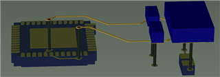
We have a board for a new design but it does not pass MII loopback at 1G.  Some of the messages go through OK, but others contain errors.  In the error messages, we have observed the RX clock increasing from 125Mhz to approximately 140MHz.  In the messages that are OK, the RX clock stays at 125Mhz.  Any ideas on what could cause this?  Any suggestion on how to resolve?

We have ran the loopback software on both an earlier design board which used a DP83867 and on a different project's board that has a DP83869HM.  The loopback works with no errors on both of these.

Thanks,

Ron

  • Hello 

    Thank you for the query.

    Can i assume the RX you are referencing is with respect to the PHY.

    The RX clock is dependent on the clock source. Can you provide more inputs on the clock source used for the PHY.

    Can you please probe the clock_out of the PHY to check if there is any variation in the clock.

    You mentioned you are able to run the loopback mode on another DP83869 design. Based on the input we can start with the assumption that the register configuration is ok.

    Regards,

    Sreenivasa

  • Yes, by RX clock, we are probing pin 32, RX_CLK on PHY.

    The clock source in this design is a 25Mhz crystal on pins 19 and 20.  We did probe on CLK_OUT and yes we saw the clock increase when writing either of the following to CLK_O_SEL in register 0x0170 "0x3 = Channel D receive clock" or "0xD  (not documented ref clock)"

    With 0xC = Reference clock (synchronous to XI input clock), it did not increase.

    I see on page 5 of https://training.ti.com/sites/default/files/docs/ti_precision_labs_-_ethernet_anatomy_of_the_phy.pdf, the RX_CLK seems to be a combination of "recovered CLK" and "local REF_CLK".

  • Sreenivasa,

      Thanks for the fast response.  Do you have any additional info on CLK_OUT when 0xD is written to CLK_O_SEL in register 0x170?  We only did it due to a response in a different thread.  We don't see this 0xD value defined in the datasheet.

    Yes, by RX clock, we are probing pin 32, RX_CLK on PHY.

    The clock source in this design is a 25Mhz crystal on pins 19 and 20.  We did probe on CLK_OUT and yes we saw the clock increase when writing either of the following to CLK_O_SEL in register 0x0170 "0x3 = Channel D receive clock" or "0xD  (not documented ref clock)"

    With 0xC = Reference clock (synchronous to XI input clock), it did not increase.

    I see on page 5 of https://training.ti.com/sites/default/files/docs/ti_precision_labs_-_ethernet_anatomy_of_the_phy.pdf, the RX_CLK seems to be a combination of "recovered CLK" and "local REF_CLK".

  • Should you need it, the following provides the configuration for the registers:

    GEN_CTRL Register (0x001F) reporting 0x0000

    GEN_CTRL Register (0x001F) writing 0x8000

    BMCR Register (0x0000) reporting 0x1140

    BMCR Register (0x0000) writing 0x0140

    RGMII_CTRL Register (0x0032) writing 0x00D0

    BMCR Register (0x0000) reporting 0x0140

    BMCR Register (0x0000) writing 0x4140

    IO_MUX_CFG Register (0x0170) reporting 0x0C0F

    IO_MUX_CFG Register (0x0170) writing 0x0D0F

    IO_MUX_CFG Register (0x0170) reporting 0x0D0F

    Secret Register (0x00C6) writing 0x0010

    GEN_CTRL Register (0x001F) reporting 0x0000

    GEN_CTRL Register (0x001F) writing 0x4000

    PHY_STATUS Register (0x0011) reporting 0xA802

  • Here is another observed observation that may help.  During an MII loopback where an error message occurs, the CLK_OUT when programed with 0xBOF  (i.e. Channel D transmit clock), also increases in frequency when a "1" bit appears on RX_D3.  However, TX_CLK (pin 29) does not, it stays at 125Mhz.  How is the Channel D transmit clock created?

  • Hello  

    Thank you for the input.

    The 0x0170 register setting is not recommended as part of the loopback tests. This continues to be default.

    Since the MII loopback tests the interface between MAC and PHY, the RJ45 cable connection is not required.

    Loopback Explanation:

    Near-End Loopback

    Near-end loopback provides the ability to loop the transmitted data back to the receiver through the digital or analog circuitry. The point at which the signal is looped back is selected using loopback control bits with several options being provided.

    When configuring loopback modes, the Loopback Configuration Register (LOOPCR), address 0x00FE, should be set to 0xE720.

    To maintain the desired operating mode, Auto-Negotiation should be disabled before selecting the Near-End Loopback mode.

    This constraint does not apply for external-loopback mode. Auto-MDIX should be disabled before selecting the Near-End Loopback mode. MDI or MDIX configuration should be manually configured.

    MII Loopback

    MII Loopback is the shallowest loop through the PHY. It is a useful test mode to validate communications between the MAC and the PHY. While in MII Loopback mode, the data is looped back and can be configured through the register to transmit onto the media.

    MII Loopback is configured using the BMCR (register address 0x0000).

    In 100Base-TX mode after MII loopback is enabled through register 0x00, it is necessary to write 0x0004 to register 0x16 for proper operation of MII Loopback.

    Please reference the below document for configuring the loopback modes ( this is similar for DP8389)

    https://www.ti.com/lit/an/snla246a/snla246a.pdf

    I am summarizing the steps generally followed 

    GEN_CTRL Register (0x001F) writing 0x8000

    BMCR Register (0x0000) writing 0x1140

    Delay control

    Please use 0X32 and 0X86 for configuring the required delays 

    Loopback Configuration Register (LOOPCR), address 0x00FE, write 0xE720.

    GEN_CTRL Register (0x001F) writing 0x4000

    Regards,

    Sreenivasa

  • Hello  

    An additional question. What is the source for the below configuration - did TI provide these ?

    Should you need it, the following provides the configuration for the registers:

    GEN_CTRL Register (0x001F) reporting 0x0000

    GEN_CTRL Register (0x001F) writing 0x8000

    BMCR Register (0x0000) reporting 0x1140

    BMCR Register (0x0000) writing 0x0140

    RGMII_CTRL Register (0x0032) writing 0x00D0

    BMCR Register (0x0000) reporting 0x0140

    BMCR Register (0x0000) writing 0x4140

    IO_MUX_CFG Register (0x0170) reporting 0x0C0F

    IO_MUX_CFG Register (0x0170) writing 0x0D0F

    IO_MUX_CFG Register (0x0170) reporting 0x0D0F

    Secret Register (0x00C6) writing 0x0010

    GEN_CTRL Register (0x001F) reporting 0x0000

    GEN_CTRL Register (0x001F) writing 0x4000

    PHY_STATUS Register (0x0011) reporting 0xA802

    Regards,

    Sreenivasa

  • Hello  

    On the register access, i have a quick note all though you might be following. Please be sure to follow the extended register access 9.4.9.1 Extended Address Space Access section.

    Regards,

    Sreenivasa

  • Hi Sreenivasa,

      Thanks for the additional info.  I realized I had not answered your question on the source of register configuration.  We started with Xilinx driver for DP83867, then modified to include steps from the DP83867 troubleshooting guide from TI, then added additional debugging instrumentation.  We have also tried using the LOOPCR instead of BMCR for other loopbacks, but decided to focus on MII loopback which is programmed through BMCR, not LOOPCR.

      So we did have a breakthrough over the weekend.  We have discovered removing the crystal and replacing with function generator, then the board passes the MII loopback test at 1G.  Following the DP93969HM datasheet, we have tried 36pF capacitors for CL1 and CL2, which is 2x the load capacitance of the ABM3 internal load capacitance of 18pF.  We have also tried 18pF.  It oscillates as expected at 25Mhz for both, but just seems to shift up to 27Mhz for couple clock cycles when we attempt to transmit data.   Any suggestion on what we should do different?  We are not currently using R1.  Would it make a difference in this case?

    Thanks,

    Ron

  • Hello Ron, 

    Thank you for the note.

    Regarding the crystal, depending on the layout, we ay have to consider the strap caps. I would try with a 27 or 33 pF load caps.

    Regarding the R1, is this the parallel resistor or series resistor? 

    Also if possible please probe the clock_out.

    9.3.4.1 Near-End Loopback

    LOOPCR is recommended  for all Near-End Loopback. Please try using this.

    Regards,

    Sreenivasa

  • Hi Sreenivasa,

      Thanks for your quick response.  On page 105 of the datasheet, R1 is between the XO pin on PHY and C2.  We are not currently using it.  Also, across the crystal in our design is a 1M ohm resistor, I am not sure why the designer added it. Have you seen this used before?  Our plan for today is to remove it and see how the board performs.   We will probe CLKOUT to understand the results. 

      What is "strap caps"?  Is that the "parasitic capacitance" discussed in the datasheet?

    Thanks,

    Ron

  • Hello Ron, 

    Thank you the inputs. Strap cap is a typo. It is stray or parasitic as you noted.

    R1 depends on the crystal you use. If you are using a low power crystal, adding R1 would be a good idea. Is the crystal placed near to the PHY? 

    I agree with you on removing the 1M ohm resistor and testing.

    Regards,

    Sreenivasa


  • Hi Sreenivasa,

      The crystal is as close as they could get it with the board having thru hole vias.  I don't have an exact length for the traces, I can get if needed.  The same layout used on a previous board using a DP83867 was used. It works on that board. I am thinking something changed internally on the DP83869 PHY due to the writeup in the datasheet changing.  The traces on this board are slightly long due to the XI/XO pins moving between DP83867 and DP83869.

  • Hello Ron, 

    Understand. I would assume the load caps are near to the crystal and place symmetrically with the ground connected to a plane.

    If there is a series resistor provision for X1 and X0, i would place a small value resistor and check as a debug option.

    Regards,

    Sreenivasa

  • Hello Ron, 

    Good morning.

    Since you mentioned you are referencing the DP83867, although you might be aware i wanted to remind that by default the 867 delay control for RGMII  is in align mode and in 869 By default RGMII shift mode will be activated. Both transmit and receive signals will be delayed by 2ns.

    Regards,

    Sreenivasa

  • Good Morning Sreenivasa,

      As part of early troubleshooting steps, we tried each value in the RGMII shift mode.  Did not seem to make a difference, but then that was when the crystal was still in instead of function generator. 

      We tried removing the resistor and tried 33pF caps, neither made a difference.  Question, did the internal circuit for crystal oscillator change between the 867 and 869 PHYs?  I know the pin locations changed and the writeup in the datasheet changed.

    Thanks,

    Ron

  • Hello Ron, 

    Thank you for the input. There have been improvements with the DP83869 oscillator.

    If i understand correctly, Without the loopback you do not see the crystal frequency changing - is the understanding correct?

    How about the power supplies, 

    VDDA2P5 (2.5V)

    VDDA1P8_1 - open or 1.8V ( When open, the two pins should not be shorted)

    VDDIO - 1.8V o 3.3V 

    VDD1P1 - 1.1V 

    VDD1P1 is 1V in DP83867. 

    Can you please check if all the pins have 100nF + 1uF for all the pins and 10nF + 10uF for each supply rail.

    Regards,

    Sreenivasa

  • I will check each voltage level today.  Earlier, we did look at the decoupling caps.  They are not as close to the pins as I would like to see.  As part of a troubleshooting step, we added extra decoupling caps closer by using some of the thru hole vias.  These extra caps were on the board when we used the function generator.  I was told the original caps were as close as they could get with all the thru hole vias need to route signals.  Do you know if it is possible to use the 869 with thru hole vias or should the board use blind vias to get the caps closer?

  • Just noticed you asked a question, "Without the loopback you do not see the crystal frequency changing - is the understanding correct?".  We see frequency change when RX data enters on the fail messages.  This is either loopback or when sending UDP out.  We started with UDP messages failing and using troubleshooting/debug steps noticed the same with MII loopback.  On good messages, we don't see the frequency change.

  • Hello Ron, 

    Thank you for the inputs.

    Can you please confirm the load caps are placed closed to the crystal. They do affect the performance. The load cap grounding - please check if this is through a short trace. 

    Would it be possible to share the crystal part number ?

    We typically recommend a  layer board and through hole vias for the supply decaps.

    Regards,

    Sreenivasa

  • I don't have the exact part number, but it is an abm3, https://abracon.com/Resonators/abm3.pdf.  It is the standard load capacitance of 18pF, I don't have the identifiers like temp/freq tolerance/freq stability readily available, but I can get if needed.  I think it was the 30ppm if memory serves correctly.  It is a 25Mhz.

  • Hi Sreenivasa,

    The voltages are correct, I have a question on the "10nF + 10uF for each supply rail".  The board has four each 869 PHYs on it.  The power rails each have their own layer.  Is it OK if these are combined with larger caps?  I am seeing 1.8V has five 22uF, three 2.2uF and eleven 0.1uF; 1.1 has one 22uF and one 0.1uF and 2.5 has one 22uF and one 0.1uF.  These are all in addition to the ones closer to the pins for each PHY which are:

    • VDDA2P5 (2.5V) Pins 3,9 each to 2.5V with two 2.2uF and two 0.1uF
    • VDDA1P8_1 - open or 1.8V ( When open, the two pins should not be shorted)  Pins 13 and 48 are not connected nor shorted
    • VDDIO - 1.8V o 3.3V Pins 18,30 each to 1.8V with one 2.2uF and three 0.1uF
    • VDD1P1 - 1.1V Pins 6, 31 and 39 each to 1.1V with two 2.2uF, two 0.1uF and four 0.01uF

    I realize these are not exactly the values called out in the datasheet, but I am told they were used on a previous board with four each 867 PHYs with no issues.  I am recommending if a another board layout is done, then we should use the values in the datasheet.  In addition, I am recommending the caps be placed closer to the pins, currently they are grouped together at bottom of each PHY.  I am trying to determine what we can do to get this board working.  It seems to work on two of the PHYs when we removed the crystal oscillator circuit and drive the XI with a 25MHz output from a FPGA.  The plan is to try similar on the other two PHYs.   Do you see anything wrong with this approach?

    Thanks,

    Ron

  • Hello Ron, 

    Thank you for the measurements. VDDIO are you using 1.8V or 3.3V.

    Regarding the crystal, i do not need the exact part number. Please note that if the crystal in a 4 pin type, some times customers tend to route the signal inside the crystal and it is recommended to avoid this.

    Regarding the decaps, each of the device and each pin has to be treated separately for the 100nF + 1 uF decoupling.

    Each of the device has to be treated as separate rail for 10nF + 10uF.

    These have be nearer to each device.

    Did you have a common clock for the 2 PHYs. A single clock output with buffer would be a good idea.

    The clock output is required to meet the DP83869 requirements.

    The Clock should be active before the DP83869 reset is released.

    Regards,

    Sreenivasa

  • Sreenivasa,

      Thanks for your response.  We are using 1.8V for VDDIO.  I assume you see from the crystal datasheet it is 2 pin type. Currently each PHY has it's own crystal on XI/XO.  

    Thanks,

    Ron

  • Hello Ron, 

    Thank you for the note.

    The 4 PHYs have 4 crystals and are all the 4 PHY layouts somewhat identical.  Are all the PHYs showing similar behaviour ?

    How is the reset controlled for all the devices ? Could you please check if the below timing is being followed.

    Could you also check if the power supply meets the below requirements 

    Regards,

    Sreenivasa

  • Hello Ron, 

    Have you considered using a single crystal oscillator and buffering the output to the PHYs.

    Regards,

    Sreenivasa

  • Hi Sreenivasa,

      I asked about doing a similar approach early on and had some push back considering redundancy.  At the time, I was thinking of using CLK_OUT of one to drive the next, which would lead to cost savings of not needing a crystal for other 3 PHYs.  Concern was if one goes down, then all would go down. 

      It is still a mystery why we cannot get 869 PHY to work with a crystal, but it works good when we use a function generator instead of the crystal.  The similar crystal circuit works on the 867.  Would you provide more detail on the improvements made to the XI/XO circuit internal to the 869?

    Thanks,

    Ron

  • Hello Ron, 

    Thank you for the reply.

    The DP83867 clock input range was limited to 1.8V irrespective of the IO voltage. This called for a clock divider when external oscillator was used and the  IO was 3.3V. We do not need a cap divider with the DP83869.

    Would it be possible to share the crystal layout. Have you had a chance to try with some alternate crystal to rule out a specific crystal issue?

    I am not sure if i am missing the inputs, did you measure the clock out and are you seeing the frequency change?

    Regards,

    Sreenivasa

  • Our board layout using the 869 is as follows, similar layout using 867 works.  The only difference in the layouts are XI/XO pin (14/15 vs 19/20)  locations.  On 867, the trace lengths are ~75 mils shorter.


    The schematic is as follows.  It works using 867.  It does not work using the 869, we tried capacitors ranging from the 18pF up to 33pF.  We have also removed the 1Mohm resistor. We have also tried a different crystal and have tested on multiple PHYs.


    We did configure the CLK_OUT and look at the output.  When configured to output 25Mhz, we don’t see the shift.  However, when CLK_OUT is configured to output 125Mhz, we do see the shift in frequency when data is being transmitted (MII loopback).


    Again, our decoupling caps are not in the best location on this layout.  However, on one of the PHYs, we have dead bugged additional caps very close to the pins.  When we replace the crystal with a function generator, the PHYs work with or without the additional caps.   When using the crystal,  we have about 40% error messages.  An error message has the frequency shift, good messages do not have the frequency shift.


    Thanks for your help and supporting us as we seek root cause,

    Ron

  • Hi Sreenivasa,

      In answer to your previous question, both the power up timing and the reset  meet the datasheet requirements.  All four PHYs show similar behavior.  Some are worst than others.

  • Hello Ron, 

    Thank for the layout.

    I see a number of vias close to the crystal routing. Are these all ground vias ?

    Also where are the load caps connected ? Did you trying putting a series resistor on the Xi and Xo  pins ?

    Regards,

    Sreenivasa

  • Hello Sreenivasa,

    The crystal and 1M ohm resistor are on pads at bottom.  Just above are the four pads for the two capacitors (CL1 and CL2 in figure 110 of datasheet). The 6 pads above those are  decoupling caps for the 1.1V.  One side would connect to the ground plane, the other side to 1.1V plane.  Above those is R575, which connects between ground and pin 12 (RBIAS) on PHY.  Above R575 is R13 which is pullup to 1.8v for MDIO(pin 41 on PHY).  Near top of traces to right are three vias under the PHY (U4 on layout) which are connected to ground.  The via under the start of the “U” on U4 connects to pin 9 on PHY, going to 2.5V plane.

    Does this answer your questions?  I need to check with the team if a series resistor was added (and value used) as a step in our troubleshooting steps. Currently it is not there. What value would you recommend for the series resistor?

    Thanks,

    Ron

  • Hello Ron, 

    Thank you for the input.

    The crystal is on the bottom side and the 1M is on the top side connected to the crystal trough vias on the crystal pads.

    The load caps seem to be after the crystal. Have you tried moving the crystal.

    Can you make use of these two resistor  pads to solder the crystal and test.

    I would add a 47R series resistor to test.

    Regards,

    Sreenivasa

  • Hi Sreenivasa,

      Thanks for the response.   The crystal and caps are on the top side.  The PHY and 1M ohm resistor are on bottom.  See following 3-D diagram:

    I am not sure what you mean by "moving the crystal".  Putting it where the 1M resistor was located moves the crystal farther from the PHY.  I don't believe having the crystal between PHY and caps would make a difference from my understanding of electronics.  Am I missing something?

    Thanks,

    Ron

  • Sreenivasa,

    I am sharing a couple O'scope captures, maybe you will see something that I am missing.  Both are using MII loopback.  Due to how we need to probe such a small part, we have cross talk on probes from the 125Mhz. Following is a successful message:

    And following is same setup, but had an error in message:

  • Hello Ron, 
    Thank you for the picture. I see a typo in my pervious message.

    The load caps seem to be after the crystal. Have you tried moving the load caps nearer to the crystal.

    Can you make use of these 1M resistor  pads to solder the load caps and do a quick test.

    Regards,

    Sreenivasa

  • Hi Sreenivasa,

      With a function generator providing 25Mhz clock into XI, the PHY passes both MII loopback and can send and receive UDP packets.  We added a white wire to the board and reprogrammed a FPGA to allow an output from the FPGA provide the 25Mhz clock to XI.  We have discovered this allows the MII loopback to pass, however it will not auto-negotiate to allow UDP packets to be sent.  In this configuration, power is applied before the 25MHz clock is available.  We have tried doing a hardware reset after the 25Mhz clock was up, but the PHY still will not auto-negotiate.  Any suggestions?

    Thanks,

    Ron

  • Hello Ron, 

    Thank you for the reply. 

    FPGA clock frequency

    Can you measure the clock frequency at the clock_out pin. The frequency is expected to match the crystal specifications in terms of accuracy and value.

    Using IO_MUX_CFG Register (Address = 0x170) you can program different frequencies. Can you please check the frequency.

    Did you have a chance to move the load caps near to the crystal ( using the 1M pads) and perform some tests.

    Regards,

    Sreenivasa

  • Hi Sreenivasa,

      We measured and confirmed the XI input met the specifications in the table above last Friday.  We made a discovery yesterday, on voltage level.  Turns out while we programed the FPGA for 1.8 volts out, it is outputting 2.5v which exceeds the max high level voltage for IX input.  We are working to correct.  Could this cause the loopback to pass, but auto negotiation to fail?

      We still don't understand why using the crystal per our original design fails.  Following the crystal manufacture's suggestion, we placed a POT in series on crystal input. This led to that PHY no longer passing loopback testing, but still see activity on LED.  We still have 3 other PHYs on that board, one connected to function generator, one connected to FPGA and one still in our original design configuration with a crystal.

    Ron 

  • Hello Ron, 

    Thank you for the inputs.

    Accurate clock is required for the MDI interface since this clock is the reference for the data transfer. With the 2.5V clock applied and vddio being 1.8V, i assume the clock is being distorted causing the MDI interface error.

    Since the loopback on the RGMII has clock reference, the deviation is the clock is not affecting the performance.

    Sorry to ask you again, Did you have a chance to move the load caps near to the crystal ( using the 1M pads) and perform some tests.

    Regards,

    Sreenivasa

  • Hello Ron, 

    Couple of questions 

    1. You mentioned that the DP83867 works but DP83869 does not work - Is the DP83867 replaced with DP83869 on the same board ?

    2. You mentioned there are 4 devices on the board. Does all the 4 devices have almost similar layout

    Regards,

    Sreenivasa

  • Hi Sreenivasa,

       Thanks for your response.  We have created work instructions to move the load caps as previous discussed, but waiting on a tech to make the update.  It will be tomorrow before one is available.  It is difficult to work virtual and solder at same time. :-)   In the meantime, we decided to increase the function generator voltage to 2.5V for one PHY connected to see if we could get a failure at the higher voltage.  Turns out it continues to work on the one PHY we tried.  That PHY is also the one we added additional decoupling caps in a previous troubleshooting step.  I am considering repeating this test on a PHY without the additional decoupling caps, but that requires someone to solder wires. 

      The pinouts are different between the 867 and 869.  Otherwise we would not have done a new board spin.  The changes from the 867 board to the 869 board are to accommodate the pin out changes.

      Yes, all four devices on board have similar layout.

      Thanks for your help as we continue to work through this.

    Regards,

    Ron

  • Hello Ron, 

    Thank you for the inputs.

    Not sure if the FPGA  output could be current limited compared to the function generator causing distortion. Is there a way you could limit the current of the function generator and test ?

    Regards,

    Sreenivasa

  • Hi Sreenivasa,

      We did think about this.  We believe the FPGA was attempting to output 2.8 volts, we measured closer to 2.5 at PHY.  Our thought was it was current limiting, so we chose to set function generator up at 2.5 volts.  We did not not want to cause internal damage to the PHY by using the full 2.8 volts.

    Ron

  • Hello Ron, 

    So if i understand correctly, the DP83867 and the DP83869 are different boards and not the same board configured for different PHYs.

    We have customers who have a common board and configure pins to suit the device.

    Was the crystal closer to the device in the DP83867 board or was this similar to what we see in the DP83869 based board.

    Regards,

    Sreenivasa

  • Hi Sreenivasa,

      Yes, two different board layouts.  One board has four 867 PHYs, the other board has four 869 PHYs.   The two board layouts have the crystal circuits and PHYs in same physical location  using similar layouts.  The difference is the XI/XO traces at the PHY had to be extended on the 869 PHYs due to pinout changing.

    Ron

  • Hello Ron, 

    Thank you for the inputs. Did the location of the PHY change with the boards.

    Is the capacitor after the crystal nearer to the PHY for the DP83867 board also?

    Regards,

    Sreenivasa

  • Hi Sreenvasa,

      I confirmed with our board layout guy.  It is the same between the 867 and 869 boards.  His words:  location of the PHY, Crystal, caps and resistor shown in the 3D model I gave you are identical between boards.

      Only difference is where the traces touch the PHY, they are longer on 869 due to pin locations moving.

    Thanks,

    Ron

  • Hello Ron, 

    Thank you. In the 3D i am seeing a rectangle picture as against square as shown in the picture attached. Any thoughts.

    Regards,

    Sreenivasa

  • Hi Sreenivasa,

      Are you referring to the ground pad (pin 49) under the PHY?  The 4.1 square on the Land Pattern Example you provided above?

    Regards,

    Ron