This thread has been locked.

If you have a related question, please click the "Ask a related question" button in the top right corner. The newly created question will be automatically linked to this question.

SN65LVDS33: CLK SI Issues @ 100 MHz

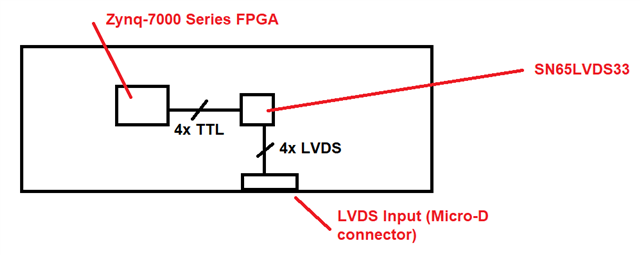
Part Number: SN65LVDS33

Hello,

We are using SN65LVDS33 to transmit 4 LVDS signals: CLK, D0, D1, and D2.

The CLK is being run at 100 MHz.

When any 2 of the 3 data channels are enabled (e.g., D0 & D1, or D0 & D2, or D1 & D2), the CLK signal integrity (SI) at the output of the receiver (i.e., the single ended side) is satisfactory.

When all 3 data channels are enabled (i.e., D0, D1, and D2), the CLK SI of the single ended signal deteriorates, and worsens as more signal edges are added to the data pattern being transmitted. The CLK SI at the input side (i.e., the LVDS side) remains good.

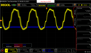
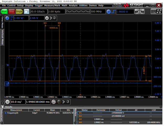
For example, if the data pattern being transmitted on all channels is 0x2222 (see image below on the left) or 0x4444 (see image below on the right), the CLK SI is good.

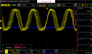
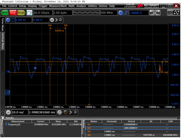
If more signal edges are added to the data pattern, e.g., 0xA9A9, the CLK SI deteriorates to the point where some cycles are missed. See image below.

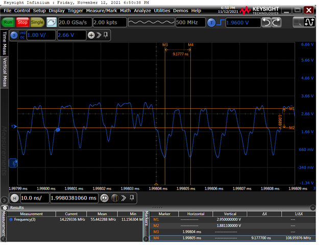
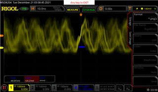
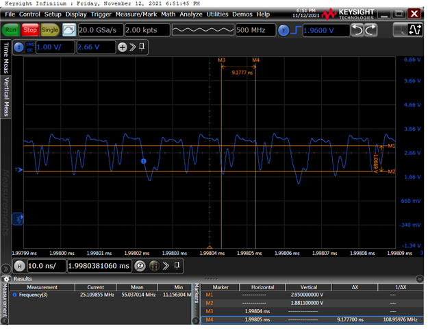
If a data pattern with constantly changing bits is transmitted, e.g., 0x5555 (image below on the left) or 0xAAAA (image below on the right), the CLK stops swinging to 0V and becomes unusable.

Are we pushing the SN65LVDS33 chip beyond its capabilities? 

All signals on the LVDS side are good. Traces are routed with the correct impedances, though they are longer than recommended by the TI app notes for LVDS signals.

Note that if we run the CLK at 50 MHz instead of 100 MHz, the CLK SI remains good across all cases.

Any feedback and/or suggestions would be appreciated.

Thanks,

Aki

  • Hi Aki,

    Correct 100MHz corresponds to 200Mbps, this is well beyond what this device can handle at its receiver. 50MHz is okay as this corresponds to 100Mbps (max data rate for this device). 

  • Hi Malik,

    Thank you for the quick response.

    However, isn't the SN65LVDS33 advertised as a 400 Mbps chip?

    According to SLAA844, SN65LVDS33 should be able to meet and exceed data rates of 400 Mbps.

    Am I missing something here?

    Regards,

    Aki

  • Hi Aki,

    My apologies, seems I have misread the part number. This device should operate at 100MHz clock. Do you happen to have a block diagram of your setup? What is the peak to peak voltage on the LVDS side?   

  • Hi Malik,

    I created a simple block diagram of the circuitry. See image below.

    The peak-to-peak voltage on the LVDS side is roughly 1V; see waveform capture below (Ch2 = green = CLK LVDS, Ch3 = blue = CLK TTL).

    Thanks,

    Aki

  • Hi Aki,

    I will look for this information however there will be delays due to US holiday this week. You should here back from me early next week at the latest. 

  • Hi Malik,

    Have you had a chance to look into this issue further?

    Thanks,

    Aki

  • Hi Aki,

    I am still looking into this issue and will follow up with you on Monday. 

  • Hi AKi,

    Sorry for the delay I was out unexpectedly on Monday. What is the state of the G/G_z pins during your testing? Also is you data DC balanced using 8b/10b or some other form of line code?  

  • Hi Malik,

    G and /G signals remain high and low, respectively, during data transmission.

    We are sending 16 bits at a time. Is DC balancing important for relatively low speeds that we are using, i.e., 100MHz? Regardless, when we alternate consecutive bits is when we get the worst clock signal; in that particular scenario, I'd assume that the data is DC balanced.

    Thanks,

    Aki

  • Hi Aki,

    It is as DC wander can still occur bit error at this low frequency range. Did you measure the LVDS signals at eh input pin's of SN65LVDS33? Do you see this issue across multiple boards/parts? 

  • Hi Malik,

    Yes, I did measure the LVDS signals at the input pins. Refer to the waveform capture shown in one of my earlier replies. The LVDS signals are good; the issue is only seen on the single ended (i.e., output) side of the chip.

    Thanks,

    Aki

  • Hi Aki,

    Do you have control of the rise time fall time of the LVDS signal? If so can you try increasing the rise time and fall time? 

  • Hi Malik,

    Unfortunately we have no control over the rise and fall times.

    Do you have any ideas why the chip wouldn't be able to drive the single-ended signals low? Is it possible that the fail-safe is being asserted?

    Aki

  • Hi Aki,

    I do not suspect the fail safe to be impact here. In fail safe condition the single ended outputs would not switch. How much current is being supplied on the board? Could you try supplying power externally to see if it helps with performance? 

  • Hi Malik,

    The 3.3V regulator can output 6.6W of power, and it is powered off the 5V rail, which in itself can output 75W. 

    We are using about 3W on the 5V rail, so I doubt current supply is the issue. When we monitor the VCC rail at the receiver, there are no dips and it's a steady 3.3V.

    Aki

  • Hi Aki,

    Would it be possible to share your schematic for review? 

  • Hi Malik,

    We can see degradation in output signal when multiple LVDS signals are driven into the chip.

    The output becomes jittery as soon as we have more than two signals which are toggling simultaneously.

    In our test, we are driving a clock at 50 MHz and N data signals with a pattern of 0x5555 synced with the clock's rising edge.

    The measurements show the output clock degradation when the number of data signals is increased

    Data Count Image
    0
    1
    2
    3

    Is this behavior expected? We would expect the buffer to be able to keep low jitter with multiple data, especially at this low speed.

    The same test, performed with 3 data at 100 Mhz gives us a very bad clock output:

    Regards,

    Laurier

  • Hi Laurier,

    This is not expected. Have you also measured the jitter in the LVDS side in the same way? Are you seeing the jitter issue on the data pins as well?  In your waveforms the output swing seems very low, could you confirm the output amplitude on the single ended-side? Would it be possible to share your schematic for review? What is kind of cable is being used on the LVDS side, is it shielded twisted pair?

  • Hi Malik,

    Have you also measured the jitter in the LVDS side in the same way?

    Yes, we measured it. It is essentially null

    Are you seeing the jitter issue on the data pins as well

    Yes, but it is less pronounced than on the clock, which runs at a higher frequency.

    In your waveforms the output swing seems very low, could you confirm the output amplitude on the single ended-side?

    Measurements where performed using a 1x probe on a 10x oscillo setting. Actual output amplitude is scaled by 10x

    Would it be possible to share your schematic for review?

    Yes, we are working on this. 

    What is kind of cable is being used on the LVDS side, is it shielded twisted pair?

    LVDS cable is twisted pair (unshielded), a little more than 2 feets. We had the issue on another generator which uses shielded LVDS twisted pair.

    The input LVDS signals follow LVDS specs (differential amplitude is on the higher end of the spec).

    We performed the same tests on a package having integrated termination resistors and one having external termination resistors with the same results.

    Regards,

    Laurier

  • Hi Laurier,

    Right now my main concern is the apparent crosstalk that is happening effecting the TTL side of the device. Is it possible to reduce the signal amplitude of the LVDS signals to see if CLK jitter is impacted? Is the CLK signal routed close to any power switching components or other high frequency signals? It is interesting that there is very little jitter on the LVDS side and single-ended data lines. I would recommend going back to the shielded twisted pair cables as these cables typically help mitigate crosstalk/radiated emissions.