This thread has been locked.

If you have a related question, please click the "Ask a related question" button in the top right corner. The newly created question will be automatically linked to this question.

TLK10232: XAUI to 10GBASE-KR Configuration

Part Number: TLK10232

Hi,

This is in continuation of the below ticket raised earlier as we haven't received a solution yet.

https://e2e.ti.com/support/interface-group/interface/f/interface-forum/1039012/tlk10232-xaui-to-10gbase-kr-configuration/3860188#3860188

This design is done consulting TI forum (ref: https://e2e.ti.com/support/interface-group/interface/f/interface-forum/531662/xaui-to-10gbase-kr-repeater-de-mux-implementation-using-tlk10232) and we are facing some challenges in getting the design up and running as indicated in the former ticket.

If TI team is not able to replicate the scenario with eval boards, can the tech support team confirm the functionality of the device TLK10232 with respect to our intended mode of operation (High-level mode of operation required is repeated again below for your reference),

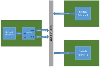
 LS -A <--> HS-A, LS-B & HS-B floating/not connected.

and switch to LS-A <--> HS-B, LS-B & HS-A floating/not connected based on PIN level or MDIO software configuration

LS Side is XAUI

HS Side is 10GBASE-KR

Regards,

Jaison

  • Hi Jaison,

    The implementation you are attempting to use should be fully allowed based on the TI product design and as per its datasheet (See below). Unfortunately, the situation has not changed in that I'm not able to replicate this setup on the bench. I'm not sure why you are encountering issue other than speculating about some unidentified error with your system software routine and/or hardware configuration.

    Excerpt from TLK10232 datasheet:

    The TLK10232 features a built-in crosspoint switch, allowing for redundant outputs and easy re-routing of data. Each output port (either high speed or low speed) can be configured to output data coming from any of the device’s input ports. The switching can be initiated through either a hardware pin or through software control, and can be configured to occur either immediately or after the end of the current packet. This allows for switching between data sources without packet corruption.

    Thanks,

    Rodrigo Natal

  • Hi Rodrigo,

    Thanks for your inputs.

    I have added a systems level block diagram our use case for a better understanding of our requirement

    Also attached is the final configuration we are doing now to get the linkup and data switch working with some work around. This work around doesn't allow faster switching as it involves link establishment every time the switching happens.

    TLK10232CTR Configuration.txt
    Address 0x18 is for channel A
    Address 0x19 is for channel B
    
    Write 0x18 0x1E 0x0000 0x8610 --> Set GLOBAL_RESET (bit 15)
    Write 0x18 0x1E 0x0000 0x3E30 --> Reset GLOBAL_RESET, Set GLOBAL_WRITE (bit 11), Set PRTAD0_PIN_EN (bit 5)
    
    Write 0x18 0x1E 0x0001 0x8B00 --> Set POWERDOWN (bit 15)
    Write 0x18 0x01 0x0096 0x0000 --> Reset LT_TRAINING_ENABLE (bit 1)
    Write 0x18 0x07 0x0000 0x2000 --> Reset AN_ENABLE (bit 12)
    
    Write 0x18 0x01 0x9000 0x024D --> TI_RESERVED_CONTROL register 
    Write 0x18 0x1E 0x8101 0x0004 --> Enable DEFAULT_TX_TRIGGER
    Write 0x18 0x1E 0x8100 0x0004 --> Trigger loading default HS TX setting values
    Write 0x18 0x1E 0x8100 0x0000 --> Trigger loading default HS TX setting values
    Write 0x18 0x01 0x9001 0x0200 --> Link train: Auto search, autotrain enabled
    
    Write 0x19 0x1E 0x0001 0x0B00 --> Reset POWERDOWN (bit 15)
    
    Write 0x18 0x1E 0x0000 0x3630 --> Reset GLOBAL_WRITE (bit 11)
    Write 0x18 0x1E 0x0017 0x3000 --> Set DST_PIN_SW_EN (bit 12) of channel-A DST_CONTROL_1
    Write 0x19 0x1E 0x0017 0x3A00 --> Set DST_PIN_SW_EN (bit 12), Set DST_PIN_SW_SRC_0 (bit [9:8]) = 10 , DST_PIN_SW_SRC_1 (bit [11:10]) = 10 of channel-B DST_CONTROL_1
    Write 0x18 0x1E 0x0019 0x3700 --> Set DST_PIN_SW_SRC_0 (bit 12), Set DSR_PIN_SW_SRC_0 (bit [9:8]) = 11, DSR_PIN_SW_SRC_1 (bit [11:10]) = 01 of channel-A DSR_CONTROL_1
    Write 0x18 0x07 0x0000 0x3000 --> Set AN_ENABLE (bit 12) of channel-A AN_CONTROL
    Write 0x19 0x07 0x0000 0x3000 --> Set AN_ENABLE (bit 12) of channel-B AN_CONTROL
    Write 0x18 0x01 0x0096 0x0002 --> Set LT_TRAINING_ENABLE (bit 1) of channel-A LT_TRAIN_CONTROL
    Write 0x19 0x01 0x0096 0x0002 --> Set LT_TRAINING_ENABLE (bit 1) of channel-B LT_TRAIN_CONTROL
    
    Write 0x18 0x1E 0x000E 0x000E --> Set DATAPATH_RESET (bit 3), TXFIFO_RESET (bit 2), RXFIFO_RESET (bit 1) of channel-A RESET_CONTROL
    Write 0x19 0x1E 0x000E 0x000E --> Set DATAPATH_RESET (bit 3), TXFIFO_RESET (bit 2), RXFIFO_RESET (bit 1) of channel-B RESET_CONTROL
    
    Workaround to bringup LS side and HS side linkup and data switch selection
    --------------------------------------------------------------------------
    
    If SW detectes Switch-A is Active (PRTAD0 = 1), 
    Write 0x19 0x01 0x0096 0x0000 --> Reset LT_TRAINING_ENABLE (bit 1) of Channel-B LT_TRAIN_CONTROL
    Write 0x19 0x07 0x0000 0x2000 --> Reset AN_ENABLE (bit 12) of Channel-B AN_CONTROL
    Write 0x18 0x07 0x0000 0x3200 --> Set AN_RESTART (bit 9) of channel-A AN_CONTROL
    Write 0x18 0x01 0x0096 0x0002 --> Set LT_TRAINING_ENABLE (bit 1) of Channel-A LT_TRAIN_CONTROL
    Write 0x18 0x1E 0x000E 0x000E --> Set DATAPATH_RESET (bit 3), TXFIFO_RESET (bit 2), RXFIFO_RESET (bit 1) of channel-A RESET_CONTROL
    Write 0x19 0x1E 0x000E 0x000E --> Set DATAPATH_RESET (bit 3), TXFIFO_RESET (bit 2), RXFIFO_RESET (bit 1) of channel-B RESET_CONTROL
    
    If SW detects Switch-B is Active (PRTAD0 = 0), 
    Write 0x18 0x01 0x0096 0x0000 --> Reset LT_TRAINING_ENABLE (bit 1) of Channel-A LT_TRAIN_CONTROL
    Write 0x18 0x07 0x0000 0x2000 --> Reset AN_ENABLE (bit 12) of Channel-A AN_CONTROL
    Write 0x19 0x07 0x0000 0x3200 --> Set AN_RESTART (bit 9) of channel-B AN_CONTROL
    Write 0x19 0x01 0x0096 0x0002 --> Set LT_TRAINING_ENABLE (bit 1) of Channel-B LT_TRAIN_CONTROL
    Write 0x18 0x1E 0x000E 0x000E --> Set DATAPATH_RESET (bit 3), TXFIFO_RESET (bit 2), RXFIFO_RESET (bit 1) of channel-A RESET_CONTROL
    Write 0x19 0x1E 0x000E 0x000E --> Set DATAPATH_RESET (bit 3), TXFIFO_RESET (bit 2), RXFIFO_RESET (bit 1) of channel-B RESET_CONTROL
    

    When only SW-B is present, then without applying workaround settings, LS-A lane alignment bit-14 in register 0x1E.000F is zero. However, as per our understanding, LS-A link can come up irrespective of HS side, Is this right?

    Only when we disable LT_TRAINING_ENABLE and AN_ENABLE on Channel-A, LS_ALIGN_STATUS bit is set, and HS-B gets selected in data-path switch.

    Regards,

    Jaison

  • Related to: When only SW-B is present, then without applying workaround settings, LS-A lane alignment bit-14 in register 0x1E.000F is zero. However, as per our understanding, LS-A link can come up irrespective of HS side, Is this right?

    • I think for LS-A link to be fully established you would need input data on LS_IN_A as well as input data on either HSRXA or HSRXB which is then deserialized and sent out to LS_OUT_A? 

    Related to: Only when we disable LT_TRAINING_ENABLE and AN_ENABLE on Channel-A, LS_ALIGN_STATUS bit is set, and HS-B gets selected in data-path switch

    • Is this a viable system level alternative for you?
    • Are you able to subsequently enable link training and have it complete successfully?

    Thanks,

    Rodrigo Natal

  • Hi Rodrigo,

    • I think for LS-A link to be fully established you would need input data on LS_IN_A as well as input data on either HSRXA or HSRXB which is then deserialized and sent out to LS_OUT_A? 

    >> SW-A & SW-B are pluggable cards and there can be scenario where both are not present and SW-B alone is plugged in once system is up. In this scenario, LS-A lane alignment should be already up and LS-A to HS-B path should get established based on the PRTAD0 line.

    • Is this a viable system level alternative for you?

    >> This will work only for our lab testing as the system need support switchover between SW-A & SW-B based on pin control. The same scheme is working in a different system where both sides are XAUI and the device used there is DS42MB200TSQ.

    • Are you able to subsequently enable link training and have it complete successfully?
    • >> Yes.

    Thanks,

    Jaison

  • Thanks for the info. I unfortunately don't have anything else to add on this item.

    Regards,

    Rodrigo Natal

  • Hi Rodrigo,

    Is it possible for the TI support team to provide us a reference configuration based on our requirement shared earlier,

    - XAUI on LS sie & 10G KR on HS side

    - 156.25MHz clock connected to REFCLK0

    - Pin level switch control based on PRTAD0.

    We can customize the DST_PIN_SW_SRC & DSR_PIN_SW_SRC fields to match with the required channels.

    We also understand that we may have to fine tune the board related parameters. But, we guess the general configuration will hold good for most of the designs.

    Thanks,

    Jaison

  • Hi Jaisson,

    Refer to the attached Excel file with an example TLK10232 KR configuration.

    Thanks,

    Rodrigo NatalNivetta_KR_Case_cfg.xlsx