


We are planning to use TLK10232 in one of our upcoming design for XAUI to 10GBASE-KR conversion plus 1:2 repeater in one direction (LS to HS) and 2:1 de-mux in the other direction (HS to LS). Prefer to use the PRTAD0 pin control for the switch selections to speed up the switching compared to MDIO.
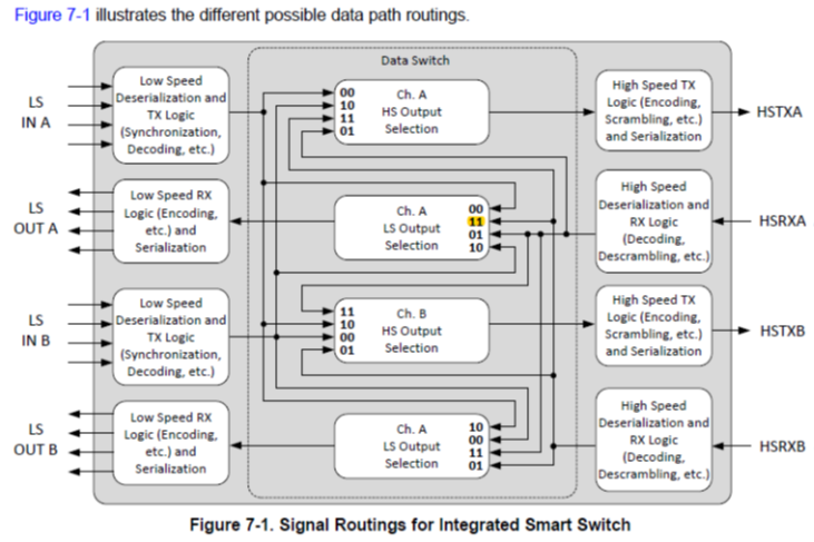
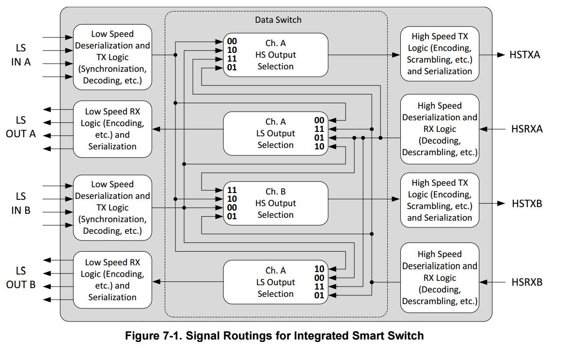
Refer to the below diagram for planned implementation,

Configuration details:
TX (LS to HS): XAUI on channel A (LSIN A) is to be replicated on both 10GBASE-KR TX (HSTXA & HSTXB) as indicated using blue connection lines.
RX (HS to LS): One of the 10GBASE-KR (HSRX) received is to be routed to XAUI channel A (LSOUT A) as indicated using green connection lines. This selection is to be done using pin control to avoid MDIO delays. The selection should be possible back and forth using the pin control. For example, LSOUT A should be able to select HSRXA or HSRXB through pin control, if the current selection is say HSRXA, it should be able to change later to HSRXB and vice versa through the pin control.
In order to configure the TLK10232 to meet the above mentioned requirements, we looked at the register descriptions and observed some conflicts and contradictions and would like to clarify this with TI support team.
Major configurations planned in TLK20232 are,
set PRTAD0_PIN_EN_SEL[2:0] to 011 (channel A RX Data switch, RX is selected since only TX or RX can be selected for pin control, TX will be under MDIO control)
set PRTAD0_PIN_EN to 0 (Input pin PRTAD0 is used for the assignment specified in 1E.0000 bits 14:12)
set DST_PIN_SW_EN to 0 (MDIO for TX)
How can we configure TLKL10232 to replicate the data on LSINA to HSTXA & HSTXB?
DST_DATA_SRC_SEL[1:0] is found common for channel A & B. Is there an option to set DST_DATA_SRC_SEL[1:0] for channel A to same channel LS input & DST_DATA_SRC_SEL[1:0] for channel B to alternate channel LS input?
Set DSR_PIN_SW_EN to 1 (pin control for RX).
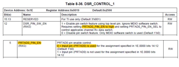
However, description for this bit is contradicting with the description given for register bit PRTAD0_PIN_EN. Here it says set PRTAD0_PIN_EN to 1 for using pin level control whereas the description for PRTAD0_PIN_EN says it must be set to ‘0’ for having pin level control. Refer below snap shots for details,
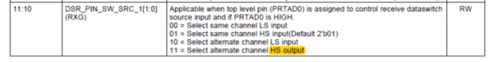
Also the source for RX switch is bit confusing. Planning to use same channel HS input when PRTAD0 is HIGH and alternate channel HS input when PRTAD0 is LOW as per the data switch diagram shown below.
However, the register description shows alternate channel HS output as one source instead of HS input.
Our main concern is whether 1:2 repeater (replication of LSINA to HSTXA & HSTXB) option is feasible or not? If this is not feasible, can we have both TX data switch and RX data switch controlled by external pin?
Thanks,
Jaison
