Part Number: TL16C752CI-Q1
Hi,
we use a TL16C752CI-Q1 in an application and we have a doubt about how works the processor interface.
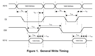
The figure 1 and 2 of the datasheet (Rev. A, which I assume is the latest revision available) show consecutive write accesses (figure 1) and read accesses (figure 2) respectively. In each figure, the first and second access sequence is different:
- the first access is controlled by an IORn or IOWn low pulse while the CSn signal is asserted
- whereas the second access is controlled by a CSn low pulse while the IORn (or IOWn) signal is asserted
I guess this implies that both types of accesses (IOWn/IORn controlled or CSn controlled) are supported by the device.
My understanding is therefore that any access begins when the last of CSn and IORn (or IOWn) goes low and ends when the first goes back high. In other words, the device detects
- the begining of an access when the logic OR of the IORn/IOWn and CSn signals goes low
- and the end of an access when the logic OR of those same signals goes high.
This makes sense considering the way the address setup and hold times (t6s and t6h) are represented.
If my understanding is correct, the timing requirements of the second access of figure 1 do not seem correctly represented as I would expect t16s and t16h to be referenced to the rising edge of CSn rather than the rising edge of IOWn. This would be consistent with the figure 2 by the way.
I would also expect t9d and t15d to be the minimum time between two valid accesses. So I would expect those timings to be represented from IORn or IOWn going high to CSn going low.
Can you please confirm that my understanding is correct and the errors in figure 1 & 2 ?
Kind regards,
Nicolas