This thread has been locked.

If you have a related question, please click the "Ask a related question" button in the top right corner. The newly created question will be automatically linked to this question.

TPS65988: About VIN_3V3 and VBUS power sequence (Dead Battery Flag)

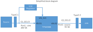
Part Number: TPS65988

I am asking title of TPS65988: About work of port1:sink, port2:source on the TPS65988DH

I tried to supply VIN_3V3 power by generated 3.3V regulator in VBUS1, and I could charge device by 5V/3A.

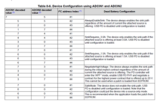
I guess to relate to “Dead Battery Flag”.

I have questions about VIN_3V3 and VBUS power sequence.

(1)My system is same time about VIN_3V3 and VBUS power sequence. Do the TPS65988 set “Dead Battery Flag” ?

(2)I want to know setting condition about “Dead Battery Flag”.

Could you tell me power up timing specification between VIN_3V3 to VBUS when the TPS65988 set “Dead Battery Flag” ?

  • Depends on the ADCIN1 and ADCIN2 configuration.

    Answer to (1): The regulator may take more time to supply power so unless confirmed, assume VBUS1 provides power to TPS65988 before VIN_3V3 arrives.

    Answer to (2): TPS65988 is powered by VBUS until dead-battery flag is cleared AND VIN_3V3 is available. Please check the table above for more information about dead-battery behavior.