This thread has been locked.

If you have a related question, please click the "Ask a related question" button in the top right corner. The newly created question will be automatically linked to this question.

TIC10024-Q1: Switching IC error issues

Part Number: TIC10024-Q1
Other Parts Discussed in Thread: TIC12400-Q1

Dear team,


This is Chris from TI Korea and one of my customers is going through an error that happened during ESD test with the switching IC. I explained in detail about the current situation, possible reasons and the questions.

1. Issue : As the picture below, when air discharge +15kV (ICU powered-up) is applied to fuse at ICU, the switching IC doesn't work. (Doesn't work with input switch).

                      ※Switching IC : TIC10024-Q1

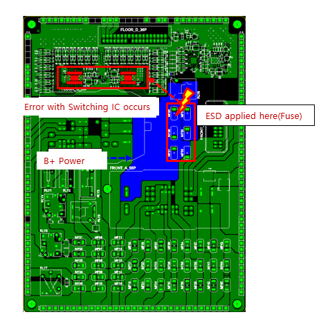
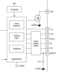
2.Possible reason : When ESD is applied, noise could be possibly applied to digital block in the switching IC and HW reset pin has been triggered.

                         Situation - 1) After the switching IC stops working, it works fine again after the battery reset.

                                           2) After ESD is applied, the register settings are reset at the switching IC.

                                           3) Works properly when ESD is directly applied to the input of switching IC.

                                           4) Increasing resistance and capacitor at switching input doesn't solve the issue.

3.Ongoing process : When serial resistor value at SPI communication line is increased from 100ohm to 390ohm, the issue is resolved.

                       → IF there is not problem with ICU function evaluation and SPI waveforms, this solution will be selected to solve the issue.

                       → After resistor is increased to 390ohm, there is no issue with the ICU function evaluation. 

4. Questions  : 1) Could possible noise in SPI communication line reset the IC's register settings? (or trigger HW reset pin)?

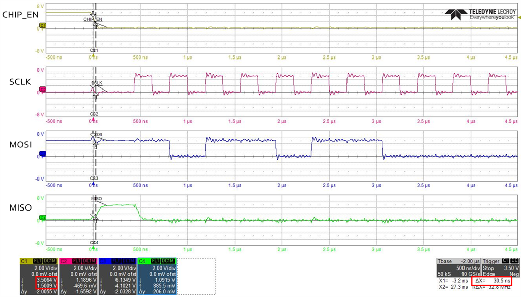
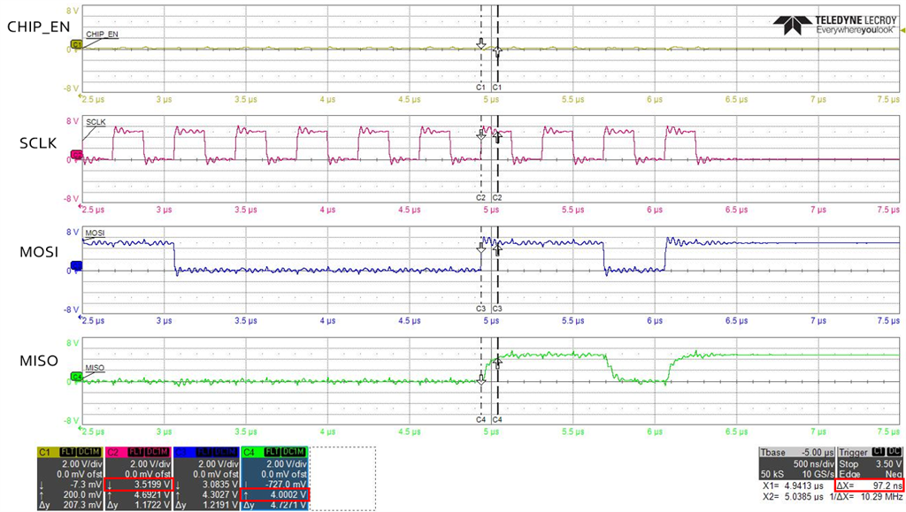
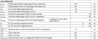
                      2) After reviewing the SPI waveform with 390ohm serial resistor, most values qualify the SPI timing parameters on datasheet, but some parameters exceed the SPI timing parameters on datasheet. Could there be possible problems with functioning or performance? (Please refer to the waveform below).

                           - t_F_CS = 30.5ns

                           - t_VALID = 97.2ns

                      3) Are there other possible reasons to this issue other than trigger in HW reset pin?

                      4) Are the read timings (Switching IC reads MOSI signal) and the read timings(MCU reads MISO) appropriate with the SCLK's falling edge?

  • Chris,

    Thanks for reaching out! We are working on getting a response for you and will get back by end of day today, Central Time.

    Best,

    Danny

  • Chris,

    Looks like you also already reached out via email for this. I believe Jonathan Nerger sent you a response about 24 hours ago. Once we get some scope shots of the RESET and supply pins, we would better be able to help you with this. It is exceptionally unlikely that a software reset is being generated by an ESD pulse. Thus, we would be determining whether this is manifesting on the VS pin, the RESET pin, or both.

    Timing characteristics are functions of the L/R/C characteristics of the circuit. The timing specifications for the TIC12400-Q1 are not based on a 390 Ω series resistor. Adding the series resistor will increase the time constant and slow down rise/fall times. Thus, the timing requirements for your microcontroller would need to fit your system with slower rise/fall times. Hopefully we can find a resolution to what's causing the reset so that the 390 Ω series resistor is not needed.

    Best,

    Danny

  • Thank you Danny,

    Could you please help answering number 4? From the waveforms I attached, the read timings of Switching IC reading MOSI signal and MCU reading MISO look appropriate with SCLK’s falling edge? 

    Thank you.

  • Chris,

    The SPI looks fine to me. The data is latched on the falling edge of SCLK, and the data must be correct 30 ns before and 20 ns after the falling edge of the clock, which seems to be the case.

    The waveform for MISO is dependent upon the L/R/C characteristics of the circuit. Timing specifications will vary from the data sheet when your 390 Ω resistor is applied.

    Were you able to get shots of VS and RESET?

    Best,

    Danny