Hello,
At my customer design, 3.3V could be applied to DS100MB203 SCL, SDA, SEL0 and SEL1 pin when VDD/VIN are off (0V).
They have a couple of questions as follows.
Q1:
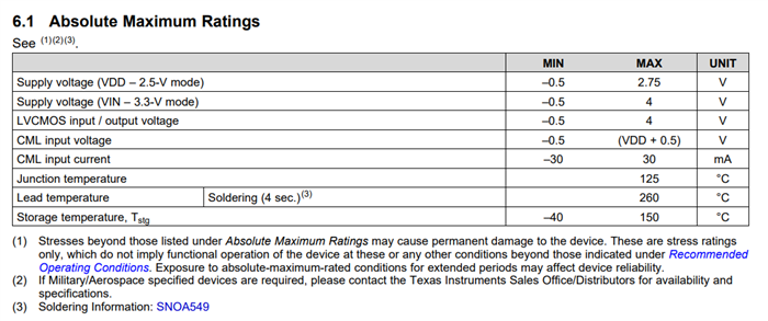
SEL0 and SEL1 are LVCMOS input pins. Since Absolute Maximum Ratings of LVCMOS input / output voltage is -0.5V to +4V, applying 3.3V to SEL0 and SEL1 when VDD/VIN=0V is OK?
Q2:
How about SCL and SDA? They could be LVCMOS input or Open drain output when VDD is on. When VDD/VIN are off, 3.3V could be applied to SCL and SDA with no damage?
Best regards,
K.Hirano

-
Ask a related question
What is a related question?A related question is a question created from another question. When the related question is created, it will be automatically linked to the original question.