Part Number: TPD6S300A
Hi team,
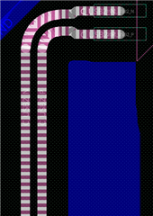
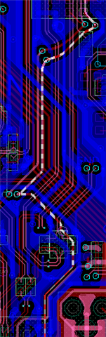
According to the datasheet layout example
The USB2.0 and SBU lines must be routed as straight as possible and any sharp bends must be minimized.
but my customer SBU line do not straight, is ok with that? 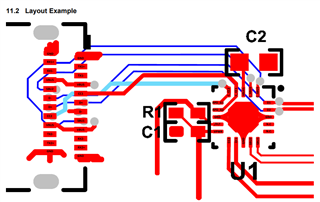
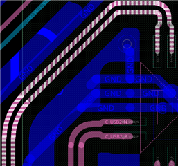
The same situation in D1/D2