This thread has been locked.

If you have a related question, please click the "Ask a related question" button in the top right corner. The newly created question will be automatically linked to this question.

SN65HVD09: Termination of unused input and output pins of SN65HVD09

Part Number: SN65HVD09

Hi,

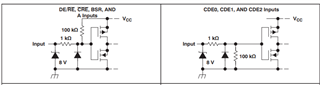
i am planning to use SN65HVD09 transceiver chip,There i am using 6 channels remaining 3 channels channels i am not going to use.So what should be done with the unused input and output pin for proper device operation.Currently i will configure unused channels as output pin using DE/RE# pin(Connect with VCC though Pull up) and also i am connected unused input pin to GND.So my input will be defined.Please clarify that this will be proper way to terminate input and outputs of the device.

Regards,

Ramesh Moorthi I.

  • As shown in the table on page 2, all pins have internal pull-up/-down resistors, so you can leave them open.

    You can save some power by using receive mode.

  • Hi Ramesh,

    According to the data sheet in one of the footnotes on page 16 and in the schematic diagrams on page 14, BSR, /CRE, A, DE, and /RE have internal pullup resistors to VCC. CDE0, CDE1, and CDE2 have internal pulldown resistors.

    If configuring RS-485 bus to outputs, then no external connection is needed and can be left floating. 

    Please let me know if you have any more questions.

    Regards,

    Tyler