This thread has been locked.

If you have a related question, please click the "Ask a related question" button in the top right corner. The newly created question will be automatically linked to this question.

TCAN4550-Q1: SSP configuration

Part Number: TCAN4550-Q1
Other Parts Discussed in Thread: TCAN4550

Hi team,

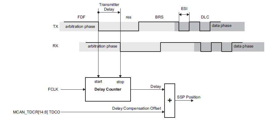
For TCAN4550-Q1, customer is confused on how to adjust secondary sample point? It seems TDCV is read only. does it mean SSP of TCAN4550 can't be adjusted by customer? 

Can you please clarify the relationship between TDCV, TDCR, TDCO and TDCF? thanks!

  • Hi Terry,

    The Transmission Delay Compensation Value (TDCV) used as the Secondary Sample Point (SSP) is selected automatically by the CAN controller in TCAN4550. The controller measures the delay between when a dominant signal is driven on m_can_tx to when the corresponding edge appears on m_can_rx, sampling every tq. This measured value is stored in the TDCV field of the Protocol Status Register (PSR address=h1044) for reference and is used during the data portion of CAN FD transmission to verify good transmission. 

    The SSP that is selected by the CAN controller can be restricted to a certain window using the Transmitter Delay Compensation Offset (TDCO) and Filter Window Length (TDCF). The offset provides extra amount of time quanta to be added to the delay measurement of the CAN controller. The filter window length defines a minimum valid delay measurement, ensuring the SSP is greater than the value defined here. These values can be configured in the Transmitter Delay Compensation Register (TDCR address=h1048). 

    Let me know if you have any more questions.

    Regards,
    Eric Schott

  • Hi Eric,

    Thanks!

    1. Can you please clarify 'the delay between when a dominant signal is driven on m_can_tx to when the corresponding edge appears on m_can_rx, sampling every tq' by picture? I can't get the point.

    2. You mean the function of SSP is to verify good transmission, so there should be a status register to show the corresponding transmission status, right? What's the register?

    3. Some CAN controller can adjust the data sample point(not for verify), whether TCAN4550 can also do it?

    4. TDCO, TDCF are protected write register, what does it mean? Can they be written by the same procedure as normal 'write register'?

  • Hi Terry,

    1. Can you please clarify 'the delay between when a dominant signal is driven on m_can_tx to when the corresponding edge appears on m_can_rx, sampling every tq' by picture? I can't get the point.

    When a signal is driven on the TXD line of transceiver (integrated in this case), there will be some delay before that same signal appears on the RXD line (also internal here). This is due to the propagation delay of the transceiver, the time it takes to drive a valid bus state, and the propagation delay of the receiver. When operating at high CAN FD speeds, this delay can be a significant amount of time quanta (tq or clock divisor period used for bit sampling). Using a secondary sample point SSP allows the CAN controller to monitor this delayed signal and ensuring it corresponds with the data it is driving on the TXD line. This effect can somewhat be represented by the image below: 

    2. You mean the function of SSP is to verify good transmission, so there should be a status register to show the corresponding transmission status, right? What's the register?

    The Protocol Status Register (address = h1044) will contain data from any error that occurred during transmission, including bit errors that would be recognized by the SSP during data phase transmission. Such an occurrence will also set the IR.PED interrupt flag to indicate a protocol error during the data phase. 

    3. Some CAN controller can adjust the data sample point(not for verify), whether TCAN4550 can also do it?

    TCAN4550 automatically selects the position for the secondary sampling point. This automatic selection can be modified with the Offset and Filter Window discussed previously. The primary sampling point is configured by the system using the Nominal and Data Bit Timing & Prescaler registers. See the linked software user's guide for more information on how to configure the primary sampling point:
    https://www.ti.com/lit/ug/sllu270/sllu270.pdf?ts=1644518234298&ref_url=https%253A%252F%252Fwww.google.com%252F 

    4. TDCO, TDCF are protected write register, what does it mean? Can they be written by the same procedure as normal 'write register'?

    In order to write to protected registers, the Configuration Change Enable bit (CCE) must be set in the CC Control Register (address = h1018). 

    Regards,
    Eric Schott