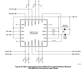
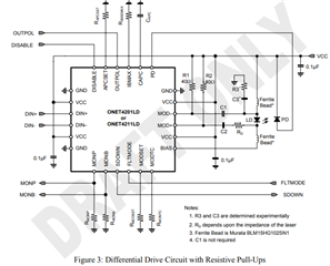
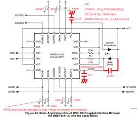
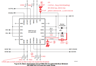
Part Number: ONET4211LD
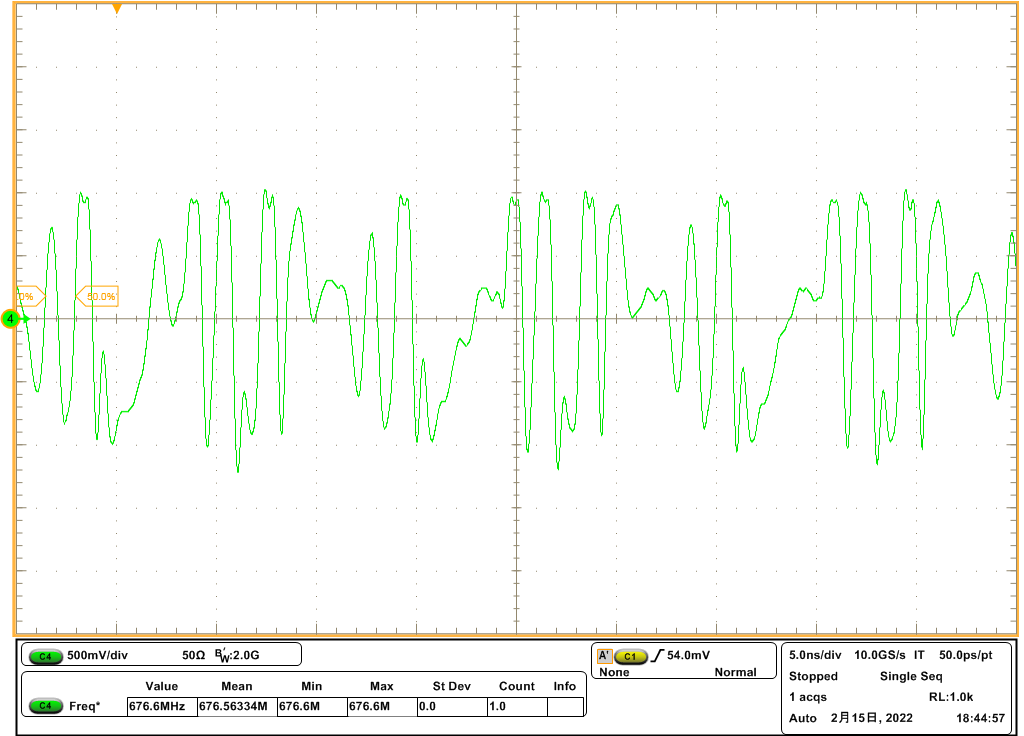
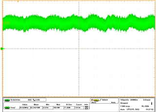
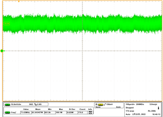
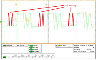
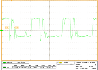
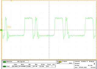
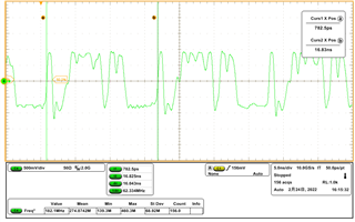
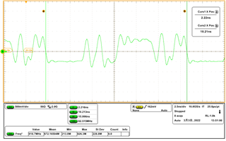
Collapse of floodlight waveform
Using ONET4211LD, make the laser diode emit light,
Checking the floodlight waveform.
* Waveform observation uses an APD module and is an oscilloscope.
We are doing it at
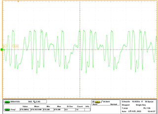
Please let me know if there is a cause for the waveform to collapse as shown in the attachment.
It looks like only a part of it has collapsed, not the whole.
(Is the following resistance setting wrong?
R MODSET: 22kΩ
R MODTC: open
R BIAS MAX: 30kΩ
R APCSET: 120kΩ
Floodlight frequency: 625MHz
Prerequisites:
-There is no abnormality in the signal input to ONET4211LD.