A related question is a question created from another question. When the related question is created, it will be automatically linked to the original question.
If you have a related question, please click the "Ask a related question" button in the top right corner. The newly created question will be automatically linked to this question.
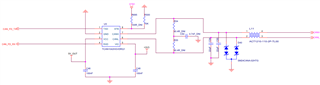
TCAN1042HGV-Q1: Can we help review schematic diagram designing ?
Pinout on schematic matches pinout on datasheet: Correct
Decoupling capacitors included and valued well: Not optimal, The datasheet recommends an additional 4.7 uF bulk capacitance placed near the main VCC supply output. The 100 nF caps you have now are good. Ensure they places as close to the VCC and VIO pins as possible.
The standby pin is good. In the current set up with R695 DNI the device will be fixed in normal mode.
The direction on TX is incorrect. It should be going into the device.
CAN Bus
Termination resistors included and valued well: It looks like R54 and R55 are DNI. If this is termination node then termination resistors are required.If this is an in-between node then they are not required as long as the stub length is short.
The split capacitor is not required but if you are going to use split termination (two 60 ohm resistors) you might as well include it. The value of the split capacitor is good.
The additional filtering capacitors are valued well.
Your CMC in not placed optimally. The CMC should be in-between the CANH and CANL pins and the termination resistors. It should be the first thing on the CAN bus. The CMC helps reduced common mode noise and all these extra components will interfere with it's performance.
The TVS diodes are good. Just ensure that they are place close and inline with the signal path.