This thread has been locked.

If you have a related question, please click the "Ask a related question" button in the top right corner. The newly created question will be automatically linked to this question.

THVD8000: Inquiry

Part Number: THVD8000

Hi,

Good Day. Customer is using the THVD8000 EVM evaluation board. He wants to connect a DC power supply to the VBB and GNB pins to send power on the line. However, the C10 and C6 in the schematic are rated for 50 and 25 V. What is the maximum DC voltage source that he can connect? Please advise. Thank you very much.

Best Regards,

Ray Vincent

  • Hi Ray,

    So if you are not modifying the board at all  25V is the highest DC power on that rail because you could have component failure.

    As for the THVD8000 itself - it really depends on the exact setup. The THVD8000 cannot handle less than -7V or greater than 12V w.r.t. ground and continue operation while the device should be protected from damage if the voltage from A to ground, B to ground, and/or A to B are with the range -18V to 18V. Generally I have seen standard applications ~24V - ~30V on average using this standard approach. The other point that needs to be considered is that the parallel impedance of all the inductors needs to be >=375 ohms to work. While higher voltage / lower power node impedance implementations are possible they are more complex than this EVM.   

    Essentially there are 12V TVS diodes connected to ground to protect the device itself. 

    If you can provide the voltage value you wish to apply as well as the needed current from the power supply, and if you have looked at a carrier frequency of theTHVD8000 if you could also provide that I will be able to better tell what needs to be changed on the EVM for your application - or if this EVM will work - as lower impedance power loads or higher voltage systems have a different implementation. 

    Please let me know!

    Best,

    Parker Dodson

  • Hi Parker,

    Good Day. Please see below the response of our customer to your reply. Thank you very much.

    I am designing a borehole geophysics tool. In my application, a 120 VDC (with 0.3 max current) is connected to a master unit (with a THVD8000 chip). The master unit is connected to a worker unit by a 2 conductor wire. This worker unit (with a THVD8000 chip) needs the 120 VDC to power itself. the digital communication between the 2 units is done with a carrier frequency of 5000 kHz. What are the modifications needed to the EVM for my application.

    Best Regards,

    Ray Vincent

  • Hi Ray,

    This is an interesting application.

    So I will preface this by saying the EVM wasn't designed with this high of a voltage in mind, so I am a bit skeptical to add that high of a DC voltage to this specific board because the protection scheme may not be robust enough. However, let me take a deeper look into the application to see if this board can be modified or what changes to overall application implementation need to be made. 

    I will look into what changes to the overall design may need to be changed - but could I also know what kind of conductor is being used and how long is distance that the THVD8000 will need to communicate along? 

    Please let me know!

    Best,

    Parker Dodson

  • Hi Parker,

    Good Day. Please see below the response of our customer to your reply. Thank you very much.

    I am testing my prototype with the EVM board but I plan to make some custom board for my application. The conductor we use is a 1000 m non isolated coax(the outer conductor is visible) cable with 80 Ohm of resistance. The capacitance between the 2 conductors is approx. 130 uF. Thank you for your time. I have tested the communication with a carrier frequency of 5000 kHz and it works great.

    Best Regards,

    Ray Vincent

  • Hi Ray,

    Thanks for the updated information!

    So after looking into it a bit deeper - this basic setup should be okay - but all the passives are going to need to change.

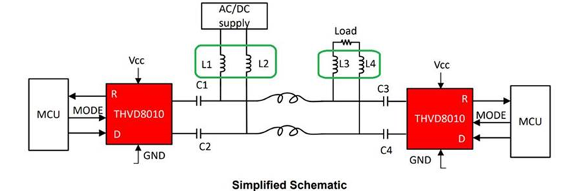
    The basic architecture of this type of application is below:

    Since there is one power source and one sink that means we treat L1 and L3 as if they were in parallel (since we assume they are AC grounded) (L2 and L4 are also treated in parallel). The total parallel impedance of the inductance needs to be 375 Ohms or greater which means all inductors need to have 750 Ohms of impedance at carrier frequency - which for 5MHz makes L = L1,2,3,4 = 23.873uH ~ 24uH minimum inductance for each inductor. 

    The capacitors should just be <= 5Ohms at carrier frequency --> C = C1,2,3,4 = 6.366nF ~ 6.4nF is the minimum capacitance you want (can have more though). 

    Since you are using a DC supply the capacitor bank on the EVM is used to not only stabilize the DC signal but help create an AC ground from the RS-485 signal. These capacitor values should be followed, but the voltage ratings will need to change to handle the 120V with capacitance derating taken into consideration. 

    There will be some reflections on the line with an 80 Ohm conductor + 120 Ohm termination - but 80 Ohm terminations are too small for RS-485 standard which could result in weaker drive strength - and at 1km it may be better to have 120 Ohm terminations. If the 1km setup has been tested and is working with 120 ohms than it should be okay. 

    The TVS diode that is on the EVM board (CDSOT23-T12C) should be able to handle the surge - but it could depend on the rise time of the DC signal (the power ratings shouldn't be violated, nor the max current but a fast rise time may cause the device to not react quickly enough) 

    That is it for the values - next is ratings.


    Based on a passive simulation with a worst case scenario (essentially 120V just appears on the bus instantaneously - which isn't realistic but it shows the extreme case  - with a slower rise time on the 120V the max ratings may not be as high). It puts ~200V across the capacitor and ~2.7A max across the inductors with a peak voltage ~120V. I will note that the inductor L1 should be the one to experience the most current at start up and C1 and C3 will take the brunt of the voltage spike. So with those ball estimates of max voltages and currents - the capacitors used must maintain a min capacitance of ~6.4nF  during normal operation and stand up without damage at max voltages - so derating of the capacitors must be taken into effect. The same story with the inductors they need to be able to handle the current spike. This is made with the assumption that the power sink is a resistive load (400 Ohms for 0.3A @120V - so whatever this load is needs to be able to handle an overshoot on the power sink during startup). 

    The diode that is use on the board has a working voltage of 12V and has a max power dissipation of 500W which is well below what it should see. From a protection point of view it should be able to handle this system - my only concern is how fast the 120V is brought on as it may be too quick for the diode to prevent damage to the IC. However with a real 120V system this may not be as big of an issue as the rise time may more closely match this diodes response curve.

    As for having the 120V DC signal powering the IC - this can be done in multiple ways there is just a few notes to follow:

    1. The THVD8000 cannot withstand more than +/-18V DC on the A and B pins - so while unpowered the A and B pins must remain between -18V and 18V w.r.t. ground. (during operation this is standard -7V to 12V for operation and -18V to 18V DC for protection). The normal setup as I described above should work for this purpose as well.

    2. The device can be powered by taking the 120V and converting into a power signal that can be used - a down SMPS is probably the best bet - depending on the wattage will guide selection on the power tree component.

    Also I do have a few notes:

    1. This board wasn't designed with typical HV clearances that other high voltage boards have - so applying high voltage to that board by prove to damage the board itself - it may be okay but it does add risk in testing (for broken boards and the like)

    2. If the system hasn't been tested at the full 1km please make sure that is done - there is some mismatch between conductor and term resistor which could cause signal integrity issues. Also the board itself should have its A/B traces at ~120 Ohms so that is something to take note when designing the board in the future as this is another source of mismatch on the board. Also as the capacitance of the cable is high for 5MHz.

    3. The unshielded conductor with its length and the carrier frequency could produce a decent amount of emissions so the layout is very important.

    Besides that it should be possible - but the inductors and capacitors need to be much more robust than what is on the current EVM as that initially ramp is going to subject them to a lot of stress. 

    I also want to include this app note: https://www.ti.com/lit/an/slla496a/slla496a.pdf?ts=1647364297681&ref_url=https%253A%252F%252Fwww.ti.com%252Fproduct%252FTHVD8000

    As it goes a bit deeper into the formulas and the design process for this part. 

    Please let me know if you have any other questions!

    Best,

    Parker Dodson