This thread has been locked.

If you have a related question, please click the "Ask a related question" button in the top right corner. The newly created question will be automatically linked to this question.

DS90UB940-Q1: mipi clock

Part Number: DS90UB940-Q1


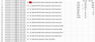
//*ds90ub940 寄存器Pattern模式:

i2ctransfer -yf 3 w2@0x2c 0x66 0x00
i2ctransfer -yf 3 w2@0x2c 0x67 0x78
i2ctransfer -yf 3 w2@0x2c 0x66 0x01
i2ctransfer -yf 3 w2@0x2c 0x67 0x12
i2ctransfer -yf 3 w2@0x2c 0x66 0x02
i2ctransfer -yf 3 w2@0x2c 0x67 0x22
i2ctransfer -yf 3 w2@0x2c 0x66 0x03
i2ctransfer -yf 3 w2@0x2c 0x67 0x00
i2ctransfer -yf 3 w2@0x2c 0x66 0x04
i2ctransfer -yf 3 w2@0x2c 0x67 0x12
i2ctransfer -yf 3 w2@0x2c 0x66 0x05
i2ctransfer -yf 3 w2@0x2c 0x67 0x02
i2ctransfer -yf 3 w2@0x2c 0x66 0x06
i2ctransfer -yf 3 w2@0x2c 0x67 0x3B
i2ctransfer -yf 3 w2@0x2c 0x66 0x07
i2ctransfer -yf 3 w2@0x2c 0x67 0xE0
i2ctransfer -yf 3 w2@0x2c 0x66 0x08
i2ctransfer -yf 3 w2@0x2c 0x67 0x61
i2ctransfer -yf 3 w2@0x2c 0x66 0x09
i2ctransfer -yf 3 w2@0x2c 0x67 0x35
i2ctransfer -yf 3 w2@0x2c 0x66 0x0A
i2ctransfer -yf 3 w2@0x2c 0x67 0x06
i2ctransfer -yf 3 w2@0x2c 0x66 0x0B
i2ctransfer -yf 3 w2@0x2c 0x67 0x04
i2ctransfer -yf 3 w2@0x2c 0x66 0x0C
i2ctransfer -yf 3 w2@0x2c 0x67 0x14
i2ctransfer -yf 3 w2@0x2c 0x66 0x0D
i2ctransfer -yf 3 w2@0x2c 0x67 0x28
i2ctransfer -yf 3 w2@0x2c 0x66 0x0F
i2ctransfer -yf 3 w2@0x2c 0x67 0x1E

i2ctransfer -yf 3 w2@0x2c 0x6a 0x22
i2ctransfer -yf 3 w2@0x2c 0x6b 0x50
i2ctransfer -yf 3 w2@0x2c 0x65 0x04
i2ctransfer -yf 3 w2@0x2c 0x64 0xE1

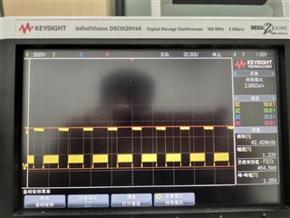
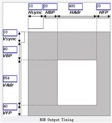
(1)940配置的pattern,接到后面的9211芯片(csi->dsi),从9211上面读取到的log来看,检测到940输出的时钟会变话,每次开机,时钟都不一样,这个是什么原因?
(2)只设置了940的pattern,而检测到前面的941(940前面的一个串行器)上面也会有信号输出,当从硬件上去掉941到940的连接引脚时,940端口却没有mipi信号输出?

  • Hi Jie Liu, 

    Thank you for your question. What exactly is your question/issue? 

    Regards, 
    Logan

  • Hi,Logan,

    As mentioned above, I would like to know the pattern of the 940 so configured, but the 9211 chip is followed from behind (CSI -->DSI) log found that mipicLock output from 940 has been changing, I wonder what is the reason?

  • Hi Jie, 

    So do below translations and interpretation correctly capture your issue? 

    (1) The pattern of 940 configuration is connected to the following 9211 chip (csi->dsi). Judging from the log read on 9211, it is detected that the clock output by 940 will change. Every time it is turned on, the clock is different. , what is the reason for this?
    (2) Only the pattern of 940 is set, and it is detected that the previous 941 (a serializer in front of 940) will also have signal output. When the connection pins from 941 to 940 are removed from the hardware, the 940 port does not. mipi signal output?

    You are doing 940 PatGen output into a CSI to DSI convert chip (9211), but MIPI CSI lock from 940 is unstable?

    Can you provide full register dump of 940 as well?
    Is the i2ctransfer the full configuration script for 940?

    Regards,
    Logan
  • yes,i2ctransfer just is the 940 pattern ,all other registers are default values

  • Hi Jie, 

    Thanks for confirming. Do you have any more information on the issue? What is 9211 reporting as CLK frequency, etc? 

    Full logs of the 940 would be useful to inspect any status, flags, errors, etc.

    Regards, 

    Logan

  • 是这样的我们公司做的一个项目从Qcom的sdm845平台出来的dsi信号经过941转LVDS后接了940转为csi又通过了LT9211转接芯片(将csi->dsi)再接到屏上,现在是从9211到屏端的数据链路正常,而配置940的pattern,如上所述,从LT9211芯片检测其输出og来看其显示的时钟一直在变化。具体log如下:

    *************LT9211 MIPI2MIPI Config*************
    LT9211 Chip ID:0x18,0x01, 0xe4
    Port A PHY Config
    Set to CSI Mode
    Input MIPI FMT: CSI_YUV422_16
    hact = 480
    vact = 854
    fmt = 0x03
    pa_lpn = 0x05
    mipi byteclk: 41052
    pixclk: 30019
    LT9211 pcr unstable!!!!
    LT9211 pcr unstable!!!!
    LT9211 pcr unstable!!!!
    LT9211 pcr unstable!!!!
    LT9211 pcr unstable!!!!
    LT9211 tx pll lock
    LT9211 tx pll cal doneStart initial panel

    Finish initial panel
    mipi output byte clock: 118749
    output pixclk: 30027
    sync_polarity = 0x00
    hfp, hs, hbp, hact, htotal = 4095 00 00 00 65535
    vfp, vs, vbp, vact, vtotal = 01 00 255 00 00

    下一次开机log

    *************LT9211 MIPI2MIPI Config*************
    LT9211 Chip ID:0x18,0x01, 0xe4
    Port A PHY Config
    Set to CSI Mode
    Input MIPI FMT: CSI_YUV422_16
    hact = 480
    vact = 854
    fmt = 0x03
    pa_lpn = 0x05
    mipi byteclk: 57291
    pixclk: 30019
    LT9211 pcr unstable!!!!
    LT9211 pcr unstable!!!!
    LT9211 pcr unstable!!!!
    LT9211 pcr unstable!!!!
    LT9211 pcr unstable!!!!
    LT9211 tx pll lock
    LT9211 tx pll cal doneStart initial panel

    Finish initial panel
    mipi output byte clock: 118749
    output pixclk: 32735
    sync_polarity = 0x0f
    hfp, hs, hbp, hact, htotal = 20 10 20 480 530
    vfp, vs, vbp, vact, vtotal = 40 10 40 854 944

    就每次开机检测 的output clock和mipi byteclk都是在变化的,这个是为什么? 

  • Hi Jie, 

    Can you provide a register dump from the 940 DES? I'd like to check the status/error registers for any clues. 

    Regards, 

    Logan

  • hi,Logan

    Do you want to see all register values for 940?

  • hi,Logan

    this is the all values for 940:

    940 chip i2c read reg 0x00 = 0x58
    940 chip i2c read reg 0x01 = 0x04
    940 chip i2c read reg 0x02 = 0x00
    940 chip i2c read reg 0x03 = 0xF0
    940 chip i2c read reg 0x04 = 0xFE
    940 chip i2c read reg 0x05 = 0x1E
    940 chip i2c read reg 0x06 = 0x00
    940 chip i2c read reg 0x07 = 0x00
    940 chip i2c read reg 0x08 = 0x00
    940 chip i2c read reg 0x09 = 0x00
    940 chip i2c read reg 0x0A = 0x00
    940 chip i2c read reg 0x0B = 0x00
    940 chip i2c read reg 0x0C = 0x00
    940 chip i2c read reg 0x0D = 0x00
    940 chip i2c read reg 0x0E = 0x00
    940 chip i2c read reg 0x0F = 0x00
    940 chip i2c read reg 0x10 = 0x00
    940 chip i2c read reg 0x11 = 0x00
    940 chip i2c read reg 0x12 = 0x00
    940 chip i2c read reg 0x13 = 0x00
    940 chip i2c read reg 0x14 = 0x00
    940 chip i2c read reg 0x15 = 0x00
    940 chip i2c read reg 0x16 = 0x00
    940 chip i2c read reg 0x17 = 0x00
    940 chip i2c read reg 0x18 = 0x00
    940 chip i2c read reg 0x19 = 0x01
    940 chip i2c read reg 0x1A = 0x00
    940 chip i2c read reg 0x1B = 0x00
    940 chip i2c read reg 0x1C = 0x23
    940 chip i2c read reg 0x1D = 0x40
    940 chip i2c read reg 0x1E = 0x00
    940 chip i2c read reg 0x1F = 0x00
    940 chip i2c read reg 0x20 = 0x00
    940 chip i2c read reg 0x21 = 0x00
    940 chip i2c read reg 0x22 = 0x00
    940 chip i2c read reg 0x23 = 0x20
    940 chip i2c read reg 0x24 = 0x08
    940 chip i2c read reg 0x25 = 0x00
    940 chip i2c read reg 0x26 = 0x83
    940 chip i2c read reg 0x27 = 0x84
    940 chip i2c read reg 0x28 = 0x20
    940 chip i2c read reg 0x2B = 0x00
    940 chip i2c read reg 0x2E = 0x00
    940 chip i2c read reg 0x34 = 0x01
    940 chip i2c read reg 0x35 = 0x00
    940 chip i2c read reg 0x37 = 0x8A
    940 chip i2c read reg 0x3A = 0x00
    940 chip i2c read reg 0x41 = 0x03
    940 chip i2c read reg 0x43 = 0x00
    940 chip i2c read reg 0x44 = 0x60
    940 chip i2c read reg 0x45 = 0x88
    940 chip i2c read reg 0x52 = 0x00
    940 chip i2c read reg 0x56 = 0x00
    940 chip i2c read reg 0x57 = 0x00
    940 chip i2c read reg 0x64 = 0xE1
    940 chip i2c read reg 0x65 = 0x04
    940 chip i2c read reg 0x66 = 0x0F
    940 chip i2c read reg 0x67 = 0x1E
    940 chip i2c read reg 0x68 = 0x00
    940 chip i2c read reg 0x69 = 0x00
    940 chip i2c read reg 0x6A = 0x22
    940 chip i2c read reg 0x6B = 0x50
    940 chip i2c read reg 0x6C = 0x00
    940 chip i2c read reg 0x6D = 0x03
    940 chip i2c read reg 0x6E = 0x00
    940 chip i2c read reg 0x6F = 0x00
    940 chip i2c read reg 0xF0 = 0x5F
    940 chip i2c read reg 0xF1 = 0x55
    940 chip i2c read reg 0xF2 = 0x42
    940 chip i2c read reg 0xF3 = 0x39
    940 chip i2c read reg 0xF4 = 0x34
    940 chip i2c read reg 0xF5 = 0x30

    and there are another strange phenomenon is when I first read the 0x69 register ,the value is 0x00; Every time after that I read  the 0x69 register,the value is 0x20; can you tell why?

    Best Regards

  • Thanks for the dumps Jie, I will review further and get back to you early next week. 

    Regards, 

    Logan

  • 嗨,洛根

    有没有任何进展?

  • Hi Jie, 

    I didn't find anything abnormal with the registers. Just to verify, this register dump was during 940 PatGen and not end to end data from upstream 941?

    Can you also provide the CSI indirect registers in 940? I'd like to make sure the CSI status registers are all correct. 

    Also, have you probed the CLK signal on scope to see if CSI CLK is stable?

    Regards, 

    Logan

  • Yes, the data of 940 is not transmitted from the 941 terminal. We only set the pattern of 940, we did not set 941.

    And what is the value of the 940 CSI indirect register? the software seems temporarily unable to read the value of the indirect register.

    And the clock on our oscilloscope is really unstable, fluctuating from 80MHz to 160MHz.

    Last but not least, what register properties do I need to configure for the initial configuration of 940 and 941?

    Best Regards

    Jie

  • Hi Jie, 

    Does the CSI sink device expect continuous or dis-continuous clock mode? If you see the CLK frequency jump around, you are probably operating in discontinuous mode. Can you provide a waveform of the CLK?

    Regards, 

    Logan

  • Csi receiver requires continuous clock input, and we have also set the clock of 940 to continuous clock

    The clock signal connected to the screen is as follows:

    /cfs-file/__key/communityserver-discussions-components-files/138/bbd4d100d418d10a1c294effa406cdca.mp4

    Don't conneted to the screen is as follows:

    The strange thing is that 940's clock is unstable when the screen is connected, and stable when the screen is not connected.

  • Hi Jie, 

    The video did not upload unfortunately. Can you summarize its issue and provide waveforms?

    What condition are the two waveforms you previously attached under? Both with device unplugged from screen? These look correct. 

    Regards, 

    Logan

  • Hi,Logan

    The two pictures above are discontinuous clocks without the output clock measured by the screen

    I'm not quite sure why the uploaded video failed, so I'll try again. The general phenomenon is that when the screen is connected, the 940 clock shows a fluctuation of 80~160Mhz

    Also, I want to know how your company's 940,941 chip is initialized and what registers need to be set? Or is it convenient to provide example code?

    Best regards 

    Jie

  • Hi Jie, 

    If you zoom out on the scope when the screen is connected, do you see the CLK switching to the low-power mode / LP11? 

    I suspect that this is what is happening, which is causing the Freq measurement to lower on the scope. 

    Regards, 

    Logan

  • hi,Logan

    Can you tell me what it means? Or what do you need me to do

    regards

    jie

  • Hi Jie, 

    After further consideration, if CLK is correctly in continuous mode, it should not leave HS active mode. 

    Taking another look at the video, the oscilloscope waveform is correct. So this might just be a weird artifact of the measurement. If not, then try to capture the part of the waveform that is deviating from the sign wave. That CLK signal looks to be correct.

    LT9211 pcr unstable!!!!
    LT9211 pcr unstable!!!!
    LT9211 pcr unstable!!!!
    LT9211 pcr unstable!!!!

    Furthermore, can you verify what PCR unstable means? What is PCR? 

    Regards, 

    Logan

  • pcr is means pixel clock recover ,According to LT9211 FAE response, this phenomenon indicates that the resolution, frame rate and other attributes output from 940Pattern are not detected

  • Jie,

    What script are you using to generate 940 PATGEN? From the scope shots the 940 output looks normal actually. Have you tried hooking up a CSI-2 generator to the 9211 directly to verify that path? How about hooking up a CSI-2 analyzer directly to the output of 940 to verify that path?

    Best Regards,

    Casey

  • hi casey

    We have tried to connect another device to 9211, and the screen can light up normally. We have verified that the link behind 940 is a path

    regards

    jie

  • Hi Jie, 

    As Casey mentioned, can you hook up a CSI analyzer to the 940 output to verify the path between the 940 and 9211? 

    Based on the 940 PatGen script, I see you are setting the following settings, can you verify this is what the 9211 is expecting:

    • 0x6A
      • Continous CLK mode
      • 2 lanes
    • 0x6B
      • OFMT: YUV422_8
      • IFMT: RGB444

    I double checked the PG script again. I found the following timings were set. Also there is currently an issue with the 0x03 RW PGCDC Pattern Generator Clock Divider Control. Currently 0 is being written to it, which isn't correct. Based on registers, you are using a 480x854 display? Is this correct? The CLK_DIV will be used to set the refresh rate / PCLK based on the display timing. Please refer to the following PG set-up guide: https://www.ti.com/lit/an/snla132g/snla132g.pdf

    Regards, 

    Logan

  • hi,logan

    We asked that 9211 FAE can support CSI continuous clock and YUV422 format. We have tested 9211 with other equipment before.

    We have changed the value of register 03 later, below are our latest configuration and screen timing


    {0x66, 0x00}, // 
    {0x67, 0x78},
    {0x66, 0x01}, // 
    {0x67, 0x12},
    {0x66, 0x02}, // 
    {0x67, 0x22},

    {0x66, 0x03}, // Pattern
    {0x67, 0x04}, // 140*(1/4)
    {0x66, 0x04}, // Total Horizontal Width
    {0x67, 0x12}, // 530
    {0x66, 0x05}, // Total Vertical and Horizontal Widths
    {0x67, 0x02}, // 944 & 530
    {0x66, 0x06}, // Total Vertical Width
    {0x67, 0x3b}, // 944
    {0x66, 0x07}, // Active Horizontal Width
    {0x67, 0xe0}, // 480
    {0x66, 0x08}, // Active Vertical and Horizontal Widths
    {0x67, 0x61}, // 854 & 480
    {0x66, 0x09}, // Active Vertical Width
    {0x67, 0x35}, // 854

    {0x66, 0x0a}, // Horizontal Sync Width
    {0x67, 0x0a}, // 10
    {0x66, 0x0b}, // Vertical Sync Width
    {0x67, 0x0a}, // 10
    {0x66, 0x0c}, // Horizontal Back Porch Width
    {0x67, 0x14}, // 20
    {0x66, 0x0d}, // Vertical Back Porch Width
    {0x67, 0x28},
    {0x66, 0x0e}, // Set Sync Polarities

    {0x67, 0x00}, 
    {0x6a, 0x22},
    {0x6b, 0x50}, 
    {0x65, 0x04}, 
    {0x64, 0xe5}, 

    Please help verify it again. Thank you

    regards

    jie

  • Hi Jie, 

    Yes, this looks correct now.

    With a CLK div of 4, you can expect a PCLK of 140MHz/4=35MHz (+/-30%). So the refresh rate will be 35MHz/944/530=~70Hz.

    I'm not sure what else we can recommend here other than analyzing the CSI output of the 940 with a CSI analyzer. PG script looks okay, and clocks/data you attached look okay. 

    Is it possible the input of the 9211 is not configured correctly?

    Regards, 

    Logan

  • hi,Logan

    Could you please tell me to configure the normal mode of 940 according to these properties on the screen?

    regards

    jie