This thread has been locked.

If you have a related question, please click the "Ask a related question" button in the top right corner. The newly created question will be automatically linked to this question.

DP83TC811R-Q1: How to understand Cin and Cout of DC CHARACTERISTICS in the datasheet?

Part Number: DP83TC811R-Q1

Hi team,

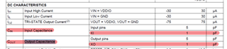
How to understand  Input Capacitance and Output Capacitance as the following capture from datasheet?

And what is the relationship between the two parameters and load capacitor of outside crystal?

I'm looking forward to your help. Thanks.

Best Regards,

Haury

  • Hi Haury,

    The Input and Output capacitance of XI, XO is the net cap load offered by the PHY.
    This capacitance contributes to some frequency shift of the crystal and the relation is non-linear.

    Typically, these Input and Output capacitances along with the board routings and loading are sent to the crystal vendor. They will analyze the loads and suggest crystal loading caps which will tune the frequency very close to 25MHz.

    --
    Regards,
    Gokul.