This thread has been locked.

If you have a related question, please click the "Ask a related question" button in the top right corner. The newly created question will be automatically linked to this question.

PCA9306: propagation time in switch mode

Part Number: PCA9306

Hi, Expert

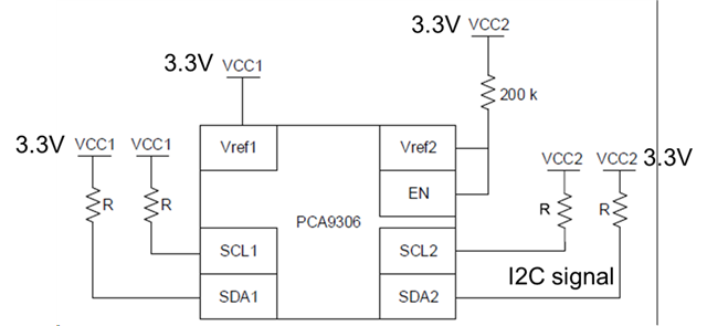
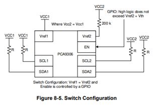
if we use PCA9306 as switch mode, the propagation time will be slightly longer than normal, so do we have the specific test result for this?

also, from other E2E answer, only the propagation time will be different in switch mode, so I want to double check with you, other parameter will don't have any effect, right?

BR

Chi

  • Chi,

    Can you post the link to the other E2E post so I can see what the engineer is talking about.

    The real addition to propagation delay in switch mode is going to be due to your MCU needing to control the EN pin. This is going to add delay time but it will be due to your MCU and how quickly your code can react. This is not a spec defined by the PCA9306.

    Best,

    Chris

  • Hi, Chris

    this is the E2E link that I take it for the reference.

    https://e2e.ti.com/support/interface-group/interface/f/interface-forum/1083483/pca9306-same-voltage-at-both-inputs-of-pca9306/4010568?tisearch=e2e-sitesearch&keymatch=PCA9306%252520Switch#4010568

    my customer's application is shown as below, Vref_1=3.3V, Vref_2 and EN through a 200k res to 3.3V. SCL and SDA transfer I2C signal. it is a level shifter design and connection, but in the real board, customer find that the signal for both side is 3.3V, so have to be used as a switch. 

    customer find that I2C communication is failed in the schematic. so want to check with you, any risk?

    BR

    Chi

  • The additional capacitance is a few pF, which does not matter for a protocol as slow as I²C.

    I do not know why I²C communication would fail. Please show oscilloscope traces of the signals.

  • Chi,

    What is the purpose of the PCA9306 in this circuit? It is not a buffer and you are not preforming any level shifting. There also is no GPIO to control the EN pin.

    I don't think there is a need for this device in your circuit and if you do require buffering or the ability to disconnect the SCL1 side from the SCL2 side this set up does not make sense.

    The PCA9306 is also only a level shifter that uses pass fet technology. It does not have the ability to ACK for another device all it will do is propagate that ACK through the I2C bus. Is the PCA9306 not able to drive the SDA line low?

    Best,

    Chris

  • Hi, Chris

    actually, this PCA9306 place holder on the board, is used as a I2C level shifter, so its layout is connected as level shifter configuration, but when customer check the system and do verification, find that the both side of PCA9306 is the same voltage 3.3V, there is no need to do voltage translation, meanwhile, customer find that we could set PCA9306 as a switch mode, so they want to use it just as a I2C switch without changing connection on board.

    this is why customer want to confirm that if there will be any risk using this schematic to do a simple switch function for PCA9306

    BR

    Chi

  • Chi,

    This is not the exact switch configuration from the datasheet. In the datasheet switch configuration is when you connect the EN pin to a GPIO pin and you control it with your MCU:

    However, in your case connecting everything to 3.3V is fine. If your set up has two different 3.3V supply rails and you would like to switch the device off when one supply rail is under powered I would recommend connecting VREF1, VREF2, and the EN pin all to the rail you expect to be powered on and off. This will control your EN pin and will isolate each side of the I2C bus from each other.

    If your devices uses one supply rail then your set up would still work but there is no reason for a PCA9306 and I would recommend removing it in the next revision.

    When you say that I2C communication is not working, is the PCA9306 able to propagate a low when you ground either SCL/SDA? Make sure that the device is still powered and VREF1,VREF2, and EN all are receiving power.

    Best,

    Chris