Part Number: DP83867IS
Hi team,
Could you please help me to answer datasheet questions below?
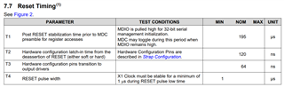
1. What is the maximum allowed value of T1, T2 and T3 in the datasheet 7.6?
(I recognize T1 requirement is already given in this thread. How about T2 and T3?)
2. After releasing reset, in order to avoid unintentional link-up before programming the register setting, my customer would like to use the POWER_DOWN pin.
Should POWER_DOWN pin be asserted low before releasing the reset signal?
Also, does POWER_DOWN pin low-to-high have any timing requirement after releasing the reset?
3. In datasheet 8.6.22, Which is the best LED_GPIO_SEL and LED_2_SEL configuration to save the power consumption? My customer will use only LED_0 and LED_1 pin.
4. In datasheet 8.6.96, Does disabling CLK_O_DISABL help to save power consumption?
5. In datasheet 8.6.97 GPIO Mux Control Register, which is the best GPIO_1_CTRL and GPIO_0_CTRL configuration to save the power consumption? My customer won't use GPIO_0 and GPIO_1.
6. Could you let me know the recommended register setting to save the power consumption? My customer would like to turn off as many circuit blocks as possible to save the power.
7. Is it OK to stop MDC clock supply when not accessing MDIO interface?
8. After stopping the MDC clock and then I want to access MDIO again, is it good if I supply MDC clock again? Does it better to wait for some time before accessing MDIO after supplying MDC clock ?
Regards,
Itoh