This thread has been locked.

If you have a related question, please click the "Ask a related question" button in the top right corner. The newly created question will be automatically linked to this question.

TCA5405: Output IO structure

Part Number: TCA5405

Hello, 

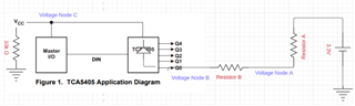
Currently I am testing the TCA5405 using the TCA7408-5405 EVM. I have modified the EVM so circuit other than the TCA5405 is not populated. 

I was testing the IC response to reverse current from GPO pin to VCC pin of TCA5405 , when VCC is off (VCC pin has 10k PD). 

The test setup is shown below. 

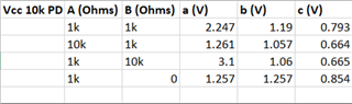
The result from the test is shown below. 

The result does not match what I expected for few reasons. 

1. The current through the resistor does not match up. The current through resistor A and B matches up, but current through the 10K PD on VCC does not match, meaning there is some other current paths. 

2. The voltage at node C is lower than expected. Taking the case where resistor A is 1k and resistor B is 0 ohm, I expected the majority of voltage to appear on node C but it didn't.

Based on the result above, I suspect there is another conduction path other than the GPO to VCC diode. 

When I conducted a diode test, I see the following values. 

  • GPO -> VCC :  0.570V
  • GND -> GPO : 0.514V
  • GPO -> GND : 1.013V

The first two diode value makes sense due to either the protection diode or MOSFET body diode. 

I also see a forward diode conduction from GPO to GND for all GPO pins. This seems odd to me and I want clarification on what this is / request for the internal GPO structure to verify. 

Sincerely, 

Tsugumi 

  • Hi Tsugumi,

    Thank you for sharing the results of your testing here. These findings are interesting to me. I need to look into this more to see if we can get a hold more information on the internal structure. I will get back to you early next week with more information. 

    Regards,
    Eric Schott

  • Hi Tsugumi,

    It seems the commonality between these two measurements is that there appears to be a current path from Vcc to GND that is not through the 10k-ohm resistor. Can you confirm that there is no other component on the board that would provide such a path? Is the Master in the figure removed? 

    Based on the information I have found, it seems that most of the back-biasing current is indeed from the MOSFETs' body diodes. Because of this, any significant positive voltage difference between the Vcc and GPO pins will result in back-biasing to the Vcc line. Because of this, we do not recommend a configuration that would have a voltage applied to the output pins while the TCA5405 is unpowered. Because the outputs of this device are always active when powered, an external biasing resistor should not be necessary for most applications. 

    Regards,
    Eric Schott

  • Hello Eric, 

    I am pretty sure I removed all components that could possibly create a path, but here are the list of components I depopulated on the EVM for you to confirm as well. 

    List of DNP : R1, R2, R3, R4, R5, R6, R7, R8, R9, U1, U2, U3, U5, U6, 

    Additionally, I ran the same test with our PCB which does not have the 10K pulldown from VCC to GND, and has no additional components on the VDD line, but this board still exhibited the 1V diode drop from OUT to GND. 

    The unknown path could be from VDD to GND as you said, but additionally it could be from OUT to GND directly. Thus, I wanted to see the internal structure so we can possibly root cause the problem. If we need to take this to offline I am more than happy to do so. 

    Sincerely, 

    Tsugumi 

  • Hi Tsugumi,

    From what I can see of the internal structure, I don't see any such path from Vcc to GND. The only section of the circuit that's not included in the section I reviewed is the ESD structure, but this doesn't seem like a likely place for such a path to exist either. 

    Is this currently causing an issue that interferes with your design? I'm curious if we might be able to look into a alternative way to combat this while searching for an internal explanation in parallel. 

    Regards,
    Eric Schott

  • Hello Eric, 

    If there is no such path from Vcc to GND, then the more I think there is a path from OUT to GND. Can you check the structure for the GPO and see if there can be a conduction path? Again, if you can send us the internal structure that will be helpful for us to confirm and verify as well. We can take this offline and sign any necessary NDA to obtain the information if necessary.  

    We currently use this chip in our design where the Vcc gets powered off while the GPO could be exposed to external voltage and thus want clear understanding of the leakage path. 

    Sincerely, 

    Tsugumi 

  • Hello Eric, 

    Any update on this item ?

  • Hi Tsugumi,

    Sorry for the delay here. 

    After reviewing this with a colleague, I think we may have identified the extra leakage path here. When the Vcc is back biased through the diode from the output pin to the supply, there are some portions of the device which partially turn on. This partially active state of the IC appears as a small load on Vcc and thus the actual voltage at Vcc appears lower than expected with the 10k-ohm pull-down. If a stronger back-bias is supplied, the voltage may raise more and more of the device may turn on, increasing the partial load on Vcc. This can therefore appear as an inconsistent load because it is dependant on the level that Vcc rises to. 

    To prevent this back-biasing from impacting other circuits that share the Vcc supply, a schottky diode may be used for the TCA5405 supply connection. While this would not stop the small leakage from the GPO to Vcc to GND, it will prevent the primary Vcc rail from rising an partially powering other ICs. 

    Regards,
    Eric Schott

  • Hello Eric, 

    Thank you for the update. 

    IC partially turning on and changing the current consumption through the 10k pulldown resistor does make sense to me. Do we have an understanding of what turns on at what voltage / current consumed by those partial internal circuits? 

    Also, is this the reason for the 1V forward drop from GPO to GND when conducting diode test? I ran the diode test using DMM from GPO to GND and then used a second DMM to measure VDD voltage, but the VDD was around 1mV which makes it hard to believe that partial internal circuit were on at this point. Thus I think there still is an internal path from GPO to GND, but was there anything internal that could cause this? 

    Additionally, if you have unencrypted SPICE model (I use LTSpice) for this chip that would be helpful for us to validate this chip further. 

    Sincerely, 

    Tsugumi  

  • Hi Tsugumi,

    The device you're inquiring about was made over 10 years ago. A lot of the design files from that time aren't around anymore. I'm also not aware of TI making unencrypted models. 

    Also, is this the reason for the 1V forward drop from GPO to GND when conducting diode test? I ran the diode test using DMM from GPO to GND and then used a second DMM to measure VDD voltage, but the VDD was around 1mV which makes it hard to believe that partial internal circuit were on at this point. Thus I think there still is an internal path from GPO to GND, but was there anything internal that could cause this? 

    I'm not 100% I follow you on this explanation. The diode test you're referring to is the one from the original post correct? And you're saying you're seeing 1V measured from the GPO to GND but have a second DMM for Vcc to GND or Vcc to GPO? 

    Have you been seeing any failures with the device during testing with our device? 

    My guess is when you did your diode testing, and saw ~0.7V on Vcc, you were basically partially powering on the device's PoR circuit since 0.7V is about half of the minimum recommended operating voltage. This is likely causing leakage through the PoR since that circuitry is mostly CMOS inputs. 

  • Hello Bobby, 

    Yes, I ran a diode test from GPO to GND using one DMM, and while having this on I measured the voltage from VDD to GND using a second DMM. I ran the test again and now I see 0.786V from VDD to GND when the GPO to GND is under diode test (with value of 1.116V) with the first DMM. When I remove the diode test , the voltage at VDD to GND drops down to 0.  This now makes more sense in that the diode test did power up the internal circuit of the IC. 

  • Hi Tsugumi,

    Are you seeing any failures/issues with the device?

    I currently still believe the extra leakage you're seeing is going from the PoR circuit since Vcc is partially powered thus leakage is going from Vcc into GND.

    -Bobby

  • Hello Bobby, 

    We do not have failures at the moment, but we were observing the reverse conduction during the validation of this chip / board with the design. 

    If there is a limit to how much reverse current the IC can handle, please advice us so we can compensate for it. 

    Sincerely, 

    Tsugumi 

  • Hi Tsugumi,

    Do you have an estimate of how much current flowing through the diode from GPO to Vcc? Currently your set up has a resistor from Vcc to GND, I assume it's not like that in your actual system.

    -Bobby

  • Hello Bobby, 

    Currently in the design, we are tweaking the resistor A and resistor B value and thus it will be nice to have the reverse current from GPO to VCC IC can handle. The 10k from VCC to GND does exist due to the other IC we have on that line. 

    Sincerely, 

    Tsugumi 

  • Hi Tsugumi,

    I believe we can refer to the clamp current values found in the absolute maximum ratings for the device's datasheet which reference a  20mA value. If the 10k resistor is present in your system, then you should be good enough to limit the current to well below that 20mA value unless you're expecting some kind of large voltage transient.

    -Bobby