This thread has been locked.

If you have a related question, please click the "Ask a related question" button in the top right corner. The newly created question will be automatically linked to this question.

TFP410: DCK abnormal

Part Number: TFP410
Other Parts Discussed in Thread: TFP401A

Dear TI-er.

My customer have a problem.

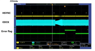
When the TFP410 of the TX stage reaches a specific temperature, the following phenomenon is observed in the RX stage.

PCB1(FPGA> TFP410) ---> HDMI Cable ---> PCB2(TFP401A> FPGA> USB)

Do you recommand the solution ? (PLL Power, layout ?)

  • Hi,

    Does this happen with one particular unit or across multiple units? 

    Can you please share the schematic and layout for review?

    Have they connected the TFP410 thermal pad to the PCB ground plane?

    Thanks

    David 

  • It is multiple units(Date code 09)

    I will be request Schematic & layout  to the customer.

    Yes. It is connected thermal pad to the PCB ground plane. but, not enough.

    Bottom side isn't thermal pad. only top side & inner layer.

    I was recommended thermal pad at bottom side.

    My customer have a question by slla131a.pdf.

    What does the following mean?

    29. Do you need to connect the PowerPAD of the TI device to ground? a. The device functions without the power pad grounded, and in most applications, connection to a thermal plane is not required for power dissipation. However, it is recommended that the power pad be grounded. Refer to SLMA002H for details on the PowerPAD technology and installation

  • Hi,

    I would point you the TFP410 datasheet

    The PowerPAD package is a 10-mm × 10-mm × 1.0-mm TQFP outline with 0,5 mm lead-pitch. The PowerPAD package has a specially designed die mount pad that offers improved thermal capability over typical TQFP packages of the same outline. The TI 64-pin TQFP PowerPAD package offers a backside solder plane that connects directly to the die mount pad for enhanced thermal conduction. For thermal considerations, soldering the backside of the TFP410 to the application board is not required because the device power dissipation is well within the package capability when not soldered. Soldering the backside of the device to the PCB ground plane is recommended for electrical considerations. Because the die pad is electrically connected to the chip substrate and hence chip ground, connecting the back side of the PowerPAD package to a PCG ground plane provides a low-inductance, low-impedance connection to help improve EMI, ground bounce, and power supply noise performance.

    You also want to make sure the solder paste coverage of the thermal pad to the ground plane is at least 50%.

    Thanks

    David

  • I provided the following data for the backside(bottom) copper pad.

    www.ti.com/.../sluu483.pdf

    My customer have a question about the link below.

    https://www.ti.com/lit/an/slma002h/slma002h.pdf

    Q) Figure 1 is heat transfer without backside copper pad.

    How I send SCH & Layout to you ?

    Plz help me.

  • Hi,

    Correct, but this is a repressive example of a PCB thermal pad design.  

    I accepted your friendship request and you can send me the board file in a private message.

    At what temperature are they seeing the failure? And are they only changing the TFP410 temperature or the entire board?

    Thanks

    David