Part Number: DP83867IS
Other Parts Discussed in Thread: DP83869
In our new design, we are using DP83867IS as 1G PHY,
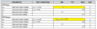
The VDDIO is set as 3.3V, The PHY CLK_OUT is interfaced with another device but it violates the DC analysis,
DP83867
VDDIO = 3.3V
VOH = 2V
VOL = 0.6V
TARGET DEVICE
VDDIO = 3.3V
VIH = 2.31V
VIL = 0.99V
NOISE MARGIN
HIGH Nh = 2-2.31 = -0.31
LOW Nl = 0.99-0.6 = 0.39
as per the calculation found the noise margin is failing,
also, we found the same VOH value in the datasheet when the VDDIO is 3.3 or 2.5V.
Could you please help to resolve this issue.