This thread has been locked.

If you have a related question, please click the "Ask a related question" button in the top right corner. The newly created question will be automatically linked to this question.

TPS65987DDK: Unable to charge battery with TPS65987 and BQ25723

Part Number: TPS65987DDK
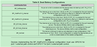
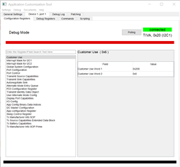
Other Parts Discussed in Thread: TPS65987D, BQ25723, BQ25703A, BQ25703, TPS65987, EV2400, TPS65988

Hello,

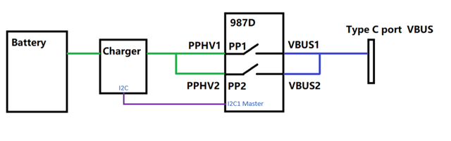
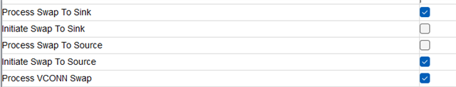
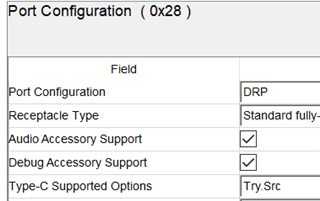
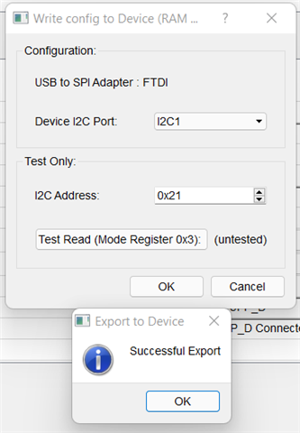
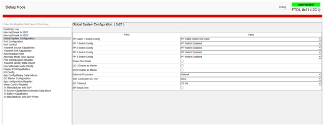
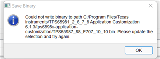
I'm not able to charge my battery 3Cells lithium by using TPS65987D and BQ25723 architecture

I,maybe, did mistake on prog or schematic.

Can you verify both please ? I put the schematic and the .pjt file configuration below 

Thank you very much,

Alan

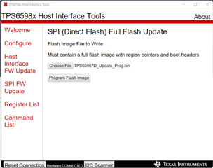
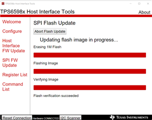
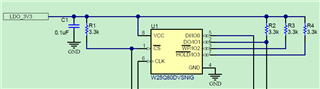
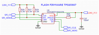
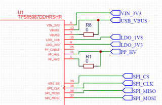
 Bidir_Alan_Prog.pjt1856.Bidirectionnal_USB_C Charger_ALAN.pdf

  • What is the application/product you are looking to build? Are you following any reference design ? 

  • I followed the Design of TIDA-01627 i just replaced the BQ25703A by BQ25723A

    I need both components to make Bi directionnal USB Charger (less or equal to 45W without MCU) in embedded product with 3cells Li-on battery 

  • And the status of the board: I can sweep I2C address of both components which are 0x21 for TPS65987D and 0x6b for BQ25723 (in the schematic we can read the ref BQ25703 but they're pin to pin compatible with BQ25723 which was mounted on the board), they're both awake but the battery doesn't charge, i think there is something wrong inside the GUI linked below but i can't find the issue

  • Thanks for the details. Passing this to an appropriate person to take this forward. 

  • Hi Alan,

    I will use your pjt to try on our EVM. By the way, I think your device is 988DH not 988DK, can you re-check?

    Bing

  • Yes, correct, but it's a 987 and yes DH not DK

  • I have also an other issue which is the following one:

    I made my program using the GUI of the application tool everything seems to work correctly. I upload the binary saved through SPI using the FTDI with the following method: "Menu Binary > Flash from current project > FTDI Region 0: 0x2000 Region 1: 0x20000" the upload is correctly done but once i go into debug mode none of my parameters set before are correctly stored even if i also try by upload with I2C through the internal ram of the device.

  • Alan, TI is closed April 15th. Engineer will get back to next week on this.

  • Hi Alan,

    I reviewed your pjt file. Have few questions below:

    1. You mentioned you need "bidirectional USB charger", I see your Port Control Register setting is "initiate swap to Source" and "process swap to source", which means that the port will always be source, to provide power to far end device.

    2. I see both inter power paths PP1 and PP2 are set as "Sink or Source" in Global System Register; and in Transmit Source Capabilities Register, PP1 used to source 5V PDO and PP2 used to source other PDOs, however, from your schematic, VBUS1 & VUBS2 are connected together, PPHV1 & PPHV2 are connected together. I'm confused about how your design your power rail? Generally, according to our EVM, if bidirectional use is needed, one PP is used as Sink Path and the other PP is used as Source Path, such as PP1 as Sink Path, PP2 as Source Path. When power flows in, it will go through PP1; when power flows out, it will go through PP2.

    Thanks.

    Bing

  • Hello Bing,

    Thank you for your answer, i need to be much clearer on the use case.

    The scope of this charger is to be integrated in portable audio spearker, inside it there is only 1 Battery and 1 USB_C connector and the power will transit only in one direction either i'm charging the speaker with a charger or i'm charging a small device using the speaker battery cell. It's the same use case than a USB C connector on a laptop for example.

    in your EVM the USB side Vbus 1 and 2 of the power rail are already connected together but the system side is not following the same use case than me. I maybe did a mistake and misunderstanding something, but if you have only 1 battery you will have to connect PP1 and PP2 because they will share the same power rail.

    For the programming files i did multiple test but i think that i did some mistakes, i would like to program it following the use case described above.

    Can you help me on this subject ?

    Thank you

    Best regards

    Alan

  • Hi Alan,

    I draw a simple block diagram for your design, please check. And you can modify it.

    If this is the design you have, I think you may need the charger to control the power flow. The 987D can indicate the power role of the Type C port, and the charger needs to determine the power flow according to this power role.

    Besides, I see there are four source PDOs in your pjt file, 5V/ 9V/ 15V/ 20V with max power 60W. According to my understand, these four source PDOs voltage are all generated from the charger, I need to confirm how the system drive these PDOs.

    Thanks.

    Bing

  • Hi, 

    I modified the project GUI regarding your answers

    you diagram block is correct, that's the use case. The 987D will indicate to the BQ25723 through I2C bus if the USB rail is in sink or source mode regarding the Power Delivery negociation and then the BQ will switch between Buck/Boost mode to adapt the power voltage between the battery and the USB voltage negociated 

    Please see as attachment the project updated regarding your comments above

    PP1 is used as sink, PP2 is used as source, i disabled Power Duo mode in order to not have both closed at the same time (that's not the use case)

    I selected process swap to sink and initiate swap to source because what i understood is that process swap to sink will order to the TPS to be sink everytime is possible and then being source only when a small device is asking to be charged. Is it the correct options to select ?

    I have an other issue, when i'm programming the device through RAM or Flash update it's updating correctly but the behavior doesn't change and when i'm going into Debug mode i see none of my options selected correctly stored, the device is in default mode with all PP disabled.

    Could you help me on it ?

    Thank you

    TPS65987D_Update_Prog.pjt

  • modified_TPS65987D_Update_Prog.pjt

    Hi Alan,

    I update your pjt file.

    Please see the change. "Initiate to source" means if PD is not source, it will always request to swap to source. "Process to source" means if the far end device wants PD to be source, PD will accept the request. From you application, I think both sink and source with "process  swap" is more reasonable. And with the setting of "Try Source", PD here will be a weak Source. For example, if the far end is an adapter, the adapter is a strong source device, it will always be source. When a weak Source meets the strong Source, it will be a Sink. If far end is a small device needs to be powered and it is compliant product, it may be able to a dual role power device or weak Sink. When a weak Source meets a dual role power device or weak Sink, it will be a Source.

    The "priority" is as below:

    strong Source (DFP, initiate to Source, no Sink) > weak Source (DRP with Try Source, process to Source/ Sink) > dual role power device (DRP, process to Source/ Sink) > weak Sink (DRP with Try Sink, process to Source/ Sink) > strong Sink (UFP, initiate to Sink, no Source)

    Hope this will help you understand.

    For FW updating, you mean that you have flash the FW to a FLASH, and after PD load FW through the FLASH, you don't see your configuration?

    Thanks.

    Bing

  • Hello Bing,

    Very helpful and clear, thank you very much,

    Yes exactly, i can upload correctly the FW through FTDI SPI or I2C both seems to work.

    but i see no behavior change, the battery is not charging and when i go into debug mode i see none of my parameters selected. it's still in manufacturing default configuration as you can see below:

    Do you have any idea ?

    Thank you

    Best regards

    Alan

  • Hi Alan,

    After you update the FW, do you do a power reset of your board? After FW update to FLASH, you need do a power reset of 987D to make it load the new FW from the FLASH.

    Thanks.

    Bing

  • Hello Bing,

    Yes i put a High 3.3V on Hreset after the FW upload, is it correct ?

    Unfortunately, It doesn't change the fact that the TPS stays in default mode

    Thanks

    Alan

  • Hi Alan,

    I have to check if HRESET is the reset for cold reset -- the reset will reload FW through FLASH. Will get you back if I get.

    Thanks.

    Bing

  • Hello Bing,

    Did you figured out if the a 3.3V on Hreset pin is effective to boot/load the FW from SPI Flash ?

    thanks

    Alan

  • Hi Alan,

    I will be out of office till next Wednesday, and at that time I will try the feature on EVM. Can you try to do the power reset for the whole board? I mean, always keep the HRESET pin to GND, and after FLASH update completes, power off the whole board, and then power on it again. (Make the VIN_3V3 supply to PD drop down and on).

    Thanks.

    Bing

  • Hello Bing, 

    I tried the whole procedure that you described : keep Hreset to GND => power on the board => FW upload => power off and power on the board.

    the board has rebooted 3 times alone but after that, i could connect in debug mode but i see no change in the configuration 

    Thanks

    Alan

  • Bing,

    Could you check on your EVM if you could upload my project correctly ?

    Is it also possible to export my project on a binary file ? i'll try to upload it directly through your binary files (i have some issue to save the project on binary files sometimes it works sometimes not and i cannot create a new binary and write on it through the application tool)

    You can find my project as attachment

    Thank you

    Alan6825.TPS65987D_Update_Prog.pjt

  • https://e2e.ti.com/cfs-file/__key/communityserver-discussions-components-files/138/6825.TPS65987D_5F00_Update_5F00_Prog

    Hi Alan,

    The bin file cannot be saved in GUI's folder so you cannot save that. You need to save in your own folder. I generated full flash binary, you can flash it to FLASH directly through a flash tool.

    I will get back to you the test result on EVM when I back to office. 

    Thanks.

    Bing

  • Hello Bing,

    I tried to make a flash upload from you bin but it seems broken. As you can see on the screenshot below, the firmware version is: ffff.ff.ff and the allocated configuration size is 0xfffffff

    Plus, i can't upload it inside the flash memory

    I copy paste the TPS65987D EVM Backup bin file and i saved the project on it using "Low Region (Full Header)" save.

    The Binary file has been updated correctly and i could upload it inside my board but i still can see a change on the behavior of the board and i still don't find my parameters when i go in Debug mode it's still in manufacturing default configuration.

    I add also the Bin file as attachment so that you can test both project and bin file (i hope that the Zip compression will not change the Bin files data, i can't upload the bin files for security reason) 

    Thank you,

    TPS65987D_Update_Prog.zip

  • Hi Alan,

    The bin I generate is the full bin. Full bin is used to flash to FLASH directly.

    Thanks.

    Bing

  • Hi Bing, 

    I tried to update the full flash using the TPS6598x Host Interface tools with your file

    it seems to work properly but once again when i go into debug mode all my parameters are deleted and the TPS is still in manufacturing default mode, any idea ?

    I'm using the following flash which should be fully compatible: 

    W25Q80DVSSIG

    Thanks

    Best regards

    Alan

  • Hi Alan,

    I will check whether W25Q80DVSSIG is with the same SPI feature. And can you please tell me how in get into debug mode? I think you should through I2C2?

    Thanks.

    Bing

  • Hello,

    I'm going into debug mode through I2C1 but if i go in debug mode through I2C2, will it change the fact that the TPS stays in manufacturing mode ?

    I see also a strange behavior sometimes the TPS is rebooting alone several times in few seconds/minutes 

    Thanks 

    Best regards

    Alan

  • I tried to connect through I2C2 i observ the same behavior. 

    The configuration uploaded before, disapear in debug mode even when the flash upload do the 3 steps Erase Programming Verifying without any trouble.

    i downloaded the PD state machine here is the result below:

    i can read multiples lines of  : Port 0 Type-C 0x0 = SRC_STATE_DISABLED 

    I try to upload the FW in debug mode through the section "HI Firmware update" 

    But when i'm doing "read boot status" i can read "Boot FAILURE"

    Thanks

    Alan

  • Alan, this is our recommendation, can you check the application on your board?

    Thanks.

    Bing

  • Hi Bing,

    Thank you for your answer, 

    See below the flash SPI Part of my schematic, I think this is exactly what you displayed above. Please, see also the TPS65987 Side to check if the MOSI/MISO Pins between the flash and the TPS are correctly connected.

    Thanks

    Best regards

  • Hi Alan,

    The codes you flashed to SPI FLASH is based on GUI 6.1.2 or GUI 6.1.3? 

    Bing

  • Hi Bing,

    It's based on GUI 6.1.3 i tried to update the GUI since it was not working properly on 6.1.2 with my board but it doesn't change the behavior observed above

    Thanks

  • Hi Bing, 

    Any update ?

    Thanks

  • Hi Alan,

    Sorry for the delay, for 6.1.2, do you mean the file cannot work with your board? What is the symptom except for no FW issue after loading?

    6.1.2 GUI works well from my EVM if I use I2C3 as master, because on EVM I2C1 is reserved for debug. Can you also have a try, help me understand the behavior here.

    Thanks.

    Bing

  • Hello Bing,

    No problem,

    Here is the background:

    i firstly had the GUI 6.1.2 on my computer started a new project select my options and tried to upload to the board.

    I saw that i could connect with I2C1 to the board without any issue and upload the firmware through SPI connection of the FT4232

    But the switch inside the TPS always stayed openned and the battery was not charging.

    I saw that i could "force" the openning of the switch by pulling low the SPI_MISO pin but the voltage was only 5V and there was no power negociation through USB PD with CC pins

    I though that the issue was on my flash so i resoldered it change it by a new one of the same reference and even change it with the same flash reference that the EVM but without any change 

    And so i tried to update the GUI i found that the new release GUI 6.1.3 was available on T.I and so i uploaded it create a new project with the same parameters and try again to upload the configuration  but once again without any change.

    I also tried to upload the configuration by the I2C1 connection and the Debug mode but i see the same behavior, the switchs stay closed and the TPS stay in default mode with all switchs openned 

    I don't think that is a soldering default because i have the same issue on 2 boards mounted.

    I sent the schematic to you and i don't think that you found any default so i begin to be out of idea  

    I have access only to I2C1 and I2C2 but i can't test I2C3 because i didn't cabled it

    I tried to invert the SPI Wires to see if the upload continue with bad connections and i saw that when the SPI Miso and Mosi are not properly connected the FW upload is interrupted so the connection seems good

    The behavior: 

    When i power up the board i have the LDO 3V3 led which is correctly lighten and sometimes the board reboot by itself

    If i don't pull the SPI_MISO down the board stays in this mode. If I pull the SPI_MISO down the PP1 became closed and i see the LEDs of internal power of the BQ25723 lighten. I can make my battery charging by using EV2400 on BQ25723 and setting the current charge but it stuck at 10W 5V 2A (default usb charge)

    And then the board reboot again by itself

    Tell me if u need any furthers details if u need the schematic it was on one answer above

    Thanks

    Alan

  • Hi Alan,

    Do you power the board in Dead Battery Mode?

    I mean, the Type-C port of TPS65988 is the only port providing power to the board?

    Thanks

    Bing

  • Hello Bing, 

    Yes i think that the TPS Start in deadbattery mode is that an issue to upload the FW ?

    Thank you

  • Hi Alan,

    You should be able to refer to datasheet Page 44:

    We have different settings determining PD's Dead Battery Boot behavior. It is determined by ADCIN1. You should choose the write setting.

    Thanks.

    Bing

  • Hi Bing, 

    I think that i should take the BP_ECWait_Internal instead of BP_NoWait (currently this one on the board). Because the TPS needs to charge his configuration in deadbattery mode (i don't know if it's possible) and then to precise to the BQ25723 to be OTG by I2C after it the TPS will be no more in deadbattery mode and the Board should start correctly.

    So is it possible to charge the configuration in dead battery mode by choosing "BP_ECWait_Internal" ? 

    Thank you,

    Best regards

    Alan

  • Hi Alan,

    BP_NoWait should be useful. With BP_NoWait, when 5V on VBUS, PD can be powered from 5V, and starts to load FW. Did you see VBUS with 5V when you do re-connection after you flash the FW to the SPI FLASH? And what is the status of LDO_3V3? It is used to power the SPI FLASH.

    Thanks.

    Bing 

  • Hello Bing,

    Sorry for my late answer, the USB VBUS is at 5V, the LDO_3V3 is at 3.3V (powered by internal LDO through USB VBUS power)

    The internal switch remains openned.

    The internal switch became closed only when I pull down the SPI_MISO Pin (It's the default configuration)  but the charger doesn't charge the battery because the BQ25723 need to be driven by I2C From the TPS and so in default configuration, the I2C parameters aren't stored into the TPS

    So it's still an issue on the FW loading but i don't understand why when the SPI pins are correctly connected between the TPS and the Memory and i changed the memory reference to use the same than the TPS65987EVM

    Thank you

    Best regards

    Alan

  • Hi Alan,

    Not sure if you have updated your pjt configuration these days? Can you share it to me? I will try to generate the file based on 6.1.2 GUI version and test it.

    So it's still an issue on the FW loading but i don't understand why when the SPI pins are correctly connected between the TPS and the Memory and i changed the memory reference to use the same than the TPS65987EVM

    And here you mean if you disable SPI loading (on our EVM, if pull down SPI_MISO to GND, FLASH config will be disabled) right?

    Thanks.

    Bing

  • Hello Bing,

    And here you mean if you disable SPI loading (on our EVM, if pull down SPI_MISO to GND, FLASH config will be disabled) right?

    Yes Exactly 

    Not sure if you have updated your pjt configuration these days? Can you share it to me? I will try to generate the file based on 6.1.2 GUI version and test it.

    Please see below my PJT Configuration

    4762.TPS65987D_Update_Prog.pjt

    Thank you best regards

    Alan

  • Hi Alan,

    I test your pjt, and just changed the I2C Master to I2C3 as I mentioned before (988DH EVM cannot use I2C1 as master, otherwise I cannot debug it, because on EVM I2C1 is reserved for debug and connected to FTDI's I2C), and it works well with this I2C Master setting.

    Based on the setting, on the test, I2C1 is used for debugging, I2C3 is used for master.

    Based on the test result, I have new questions below:

    1. How you flash the SPI FLASH? I assume you use FTDI to flash directly right?

    2. Which I2C group do you use to enter debug mode?

    Thanks.

    Bing

  • Hello Bing,

    Based on your comments above i've made a V2 of my prototype charging board

    Is it possible for you to make a quick verification of the schematic ? (you can find it below as attachment)

    I would like also to verify the BQ25723 part should i make an other post for it ?

    Thank you very much for your support

    Best regards

    Alan

    Schematic_Bidirectionnal USB_C Charger_V2.pdf

  • Hi Alan,

    For your latest schematic, for PD controller's part, it looks good to me. For charger's part, you'd better submit a new e2e thread and label it with charger's part number, and the expert from charger's product line will give you some suggestions if needed.

    And by the way, can you please share more details about mode transition? I mean, if battery is out of power, then the board can only be Sink; and if battery is with power, (maybe not much but is yet able to power TPS65987DH through VIN_3V3), the board will always be Source. -----> Is this the expected behavior you want?

    Thanks.

    Bing

  • Hello Bing,

    Many thanks for your review,

    And by the way, can you please share more details about mode transition? I mean, if battery is out of power, then the board can only be Sink; and if battery is with power, (maybe not much but is yet able to power TPS65987DH through VIN_3V3), the board will always be Source. -----> Is this the expected behavior you want?

    Yes that's exactly the kind of behavior i'm expected.

    The board need to always be in source mode when the battery has still a bit of power to charge small devices such as smartphones or others things.

    And of course if i'm charging the board with an 220V AC charger Power Delivery which can be only source the board has to switch in sink mode to charge the battery even if the battery is still a bit charged.

    Thank you

    Best regards

  • Hi Alan,

    That's good. Because in Dead Battery Mode, the PD will limit the output PDO voltage level to 5 V. (VIN_3V3 is powered later than VBUS, the PD enters Dead Battery Mode). But now for you application, the situation may not occur, that's okay from my review.

    Thanks.

    Bing