


Part Number: DS90UB928Q-Q1
Hi team,
As you can see in the below figure, the GPIO2&3 has a short time high level. Could you kindly tell me what is the reason?
Channel 1: VDDIO&VDD33
Channel 2: GPIO2
Channel 3: GPIO3
BR
Jiawei
Part Number: DS90UB928Q-Q1
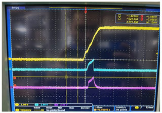
Hi team,
As you can see in the below figure, the GPIO2&3 has a short time high level. Could you kindly tell me what is the reason?
Channel 1: VDDIO&VDD33
Channel 2: GPIO2
Channel 3: GPIO3
BR
Jiawei
