Other Parts Discussed in Thread: DP83822I
Hello,
I am trying to make a 10BASE-T1L to 10BASE-T media converter circuit using the DP83TD510E and the DP83822I. I built prototypes. The RGMII is not working to pass data from the 822 to the 510. The RGMII passes data fine from the 510 to the 822. The traffic tester reports CRC and alignment errors.

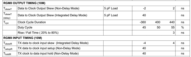
The DP83TD510E has no timing diagrams for RGMII. Looking at the timing diagrams for the DP83822I I am wondering if the problem is there is no shift on the 822 RX_CLK to 510 TX_CLK connection. The datasheets for the 2 parts indicate
- The DP83822I has no shift added to the RX_CLK, but there is a shift added to the TX_CLK.
- The DP83TD510E no shift is added to the RX_CLK, or the TX_CLK.
I have no microcontroller on the board to send MDIO commands. The PHYs are configured by straps. Here are how the straps are configured.
DP83822I :
| PIN | PIN # | Internal | Set to | DESCRIPTION |
| NAME | PU/PD | MODE | ||
| -------------------------------------------------------------------------------------------------------------------------- | ||||
| COL | 29 | PU | 4 | Internal PU - disables 100BASE-FX, set PHY addr to 00001. |
| RX_D0 | 30 | PD | 2 | External 10K PU and 2.49K PD - sets 10BASE-Te, half/full duplex, and PHY addr to 00001. |
| RX_D1 | 31 | PD | 1 | Internal PD - disables EEE, set PHY addr to 00001. |
| RX_D2 | 32 | PD | 1 | Internal PD - disables Fast Link Drop, set PHY addr to 00001. |
| RX_D3 | 1 | PD | 1 | Internal PD - sets 10BASE-Te, half/full duplex, and PHY addr to 00001. |
| LED_0 | 17 | PU | 4 | Internal PU - sets 10BASE-Te, half/full duplex. |
| CRS | 27 | PU | 1 | External 1.96K PD - configure LED_0 as Link and Activity. |
| RX_ER | 28 | PU | 3 | External 1.96K PD, 6.2K PU - enables Auto-MDIX, enables RGMII. |
| RX_DV | 26 | PD | 1 | Internal PD - Set RGMII mode with 25MHz reference clock provided at XI pin. |
DP83TD510E:
| STRAP | PIN | PIN # | Internal | DESCRIPTION |
| # | NAME | PU/PD | ||
| -------------------------------------------------------------------------------------------------------------------------- | ||||
| 1 | RX_D3 | 13 | PD | Internal PD - sets PHY address to 0000. |
| 2 | RX_D2 | 14 | PD | Internal PD - sets pin 18 as CRS_DV. |
| 3 | RX_D1 | 15 | PD | Internal PD - sets PHY to RGMII mode. |
| 4 | RX_D0 | 16 | PD | Internal PD - sets PHY address to 0000. |
| 5 | RX_DV | 18 | PD | Internal PD - sets Clockout/LED_1 pin as 25MHz clock output. |
| 6 | RE_ERR | 20 | PD | Internal PD - sets PHY address to 0000. |
| 7 | LED_2 | 28 | PD | External PU - sets APL TX/RX voltage level to prefer 1 Vpp. |
| 8 | LED_0 | 29 | PD | External PU - sets PHY to RGMII mode. |
| 9 | GPIO1 | 32 | PD | Internal PD - sets PHY address to 0000. |
| 10 | GPIO2 | 8 | NA | Mandatory PD - sets Receiver with tapping at 50 Ω. |
I'm not sure what the problem is for sure. The delay is just a guess. If you have any ideas on what might be wrong and how to figure out what it is and fix it I would love to hear them.
Thanks