


Part Number: XIO2213B
Hello,
About the XIO2213, I have some questions to confirm:
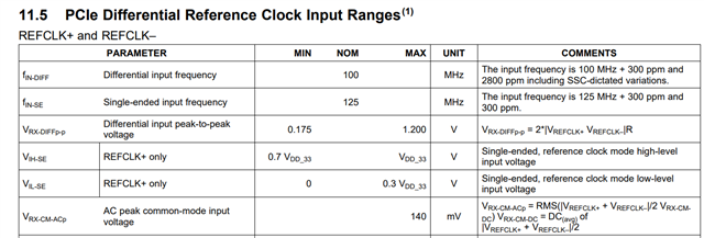
1. About the REFCLK+/REFCLK-, if it could accept 100MHz LVDS input clock. As the datasheet described, what is the common voltage of REFCLK?
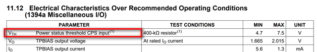
2.CPB input threshold voltage is 4.7V ~7.5V, but CPB connected 12V bus power of XIO2213EVM, so what is the maximum bus power ?
3.LPS_L and LPS_P need short connection, but they also pull down to GND of XIO2213EVM, why they need pull down?
4. CTL0/CTL1/D[7:0] are float of XIO2213EVM, I wonder if they are float, do they affect the conversion between PCIE and 1394? CTL0/CTL1/D[7:0] are the control and data bus about PHY and LLC, so I am not sure if they could float directy? Like the EVM schematic, if they could float, what are their function of CTL0/CTL1/D[7:0] ?
Best regards
Kailyn
