Part Number: XIO2213B
Other Parts Discussed in Thread: TSB82AA2
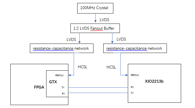
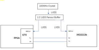
- PCIe Differential Reference Clock Input
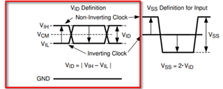
1Vid range:0.0675V~0.6V,is it right?
2What is the Vicm range? Is the LVDS level OK?
3The XIO2213B design has no internal 50-Ω-to-ground termination resistors. Both REFCLK inputs, at approximately 20 kΩ to ground, are high-impedance inputs.
Therefore, should I additionally add 50-Ω-to-ground termination resistors at these two pins?
4The following figure shows a solution of the PCI-Express Reference Clock Inputs,is it ok ?
- The XIO2213 EVM
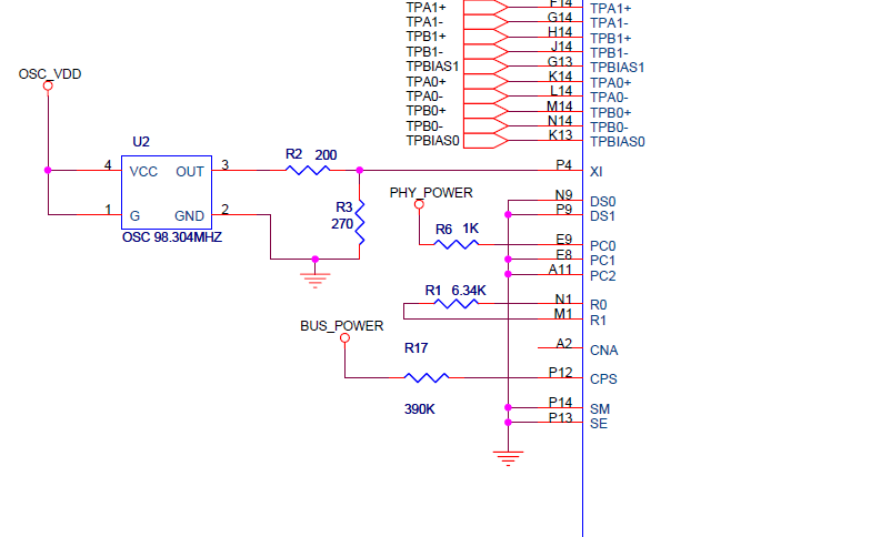
1What is the range of BUS_POWER that will not cause the voltage of the CPS exceed the XIO2213b's recommended input range?
2Why add a pull-down resistor(R15) at LPS?
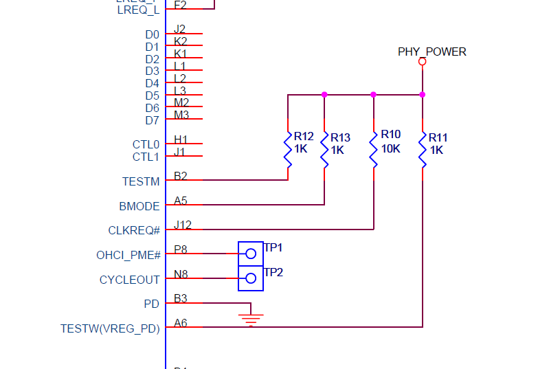
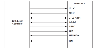
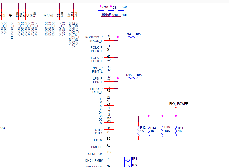
3I think XIO2213 contains LLC and PHY, so if the pins(CTL0/CTL1/D[7:0]) are not connected, will it not cause the PCI Express to 1394b translation to fail?
If the pins (CTL0/CTL1/D[7:0]) do not need to be connected and the XIO2213b is capable of PCI Express to 1394b conversion, then why does the XIO2213b pin out these pins (CTL0/CTL1/D[7:0]) and what is their usage scenario?
The reason I have this doubt is that the pins such as CLK_P, PCLK_L, LCLK_P, LCLK_L, etc. are defined in the datasheet as clock inputs and outputs between 1394 link layer and physical layer, etc. After the XIO2213b pins them out, the user needs to do the connection externally by himself;
Similarly, I just assume that the pins(CTL0/CTL1/D[7:0]), which also act as the control and data bus signals of 1394 link layer and physical layer, must also be processed to accomplish the PCI Express to 1394b translation.