This thread has been locked.

If you have a related question, please click the "Ask a related question" button in the top right corner. The newly created question will be automatically linked to this question.

DP83822I: issue in XINJE

Part Number: DP83822I


Hi Team 

Good day, and hope this email finds you well.

I’m reaching out because my customer XINJE have some question about our DP83822I.(The application is  in HMI(human machine interface))Could you please help me about these issue?

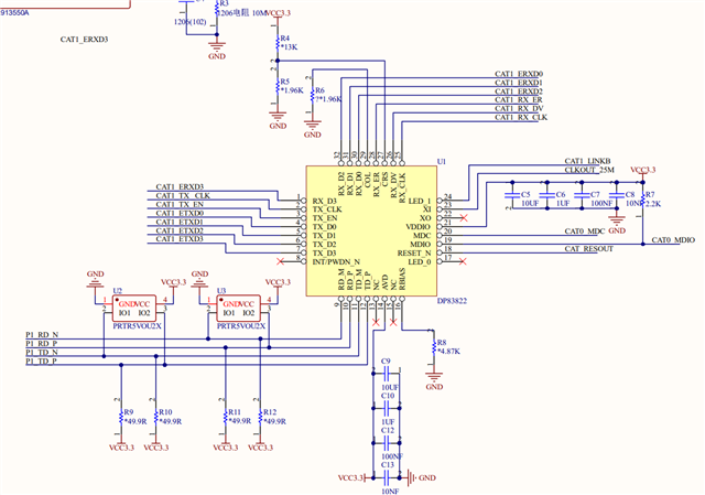
  1. They want to run it in the 100M Full-Duplex Mode (MII mode), but there is something wrong : The register flag bit-- Auto-Negotiation Complete (0X001.5) has always been 0, indicating that the chip auto-negotiation has not yet been completed. Is this issue related to their resistor configuration? Please kindly receive the attachment  of their schematic.DP83822I schematic

        2.The register marker bit--- SMI Preamble Suppression (0x0001.6) is 1, and according to the manual, the chip appears to remove the Preamble during normal operation. However, XINJE usage scenario requires that this Preamble must be retained, so they wanted to consult how to modify the configuration of this aspect. The register value of the 0x00 to the 0X1F is attached please received.

register value

        3.COL/CRS is not required in the their case of ethercat, but how to configure it does not affect the normal operation of the PHY chip. I find the COL is default  disable, so disable the COL doesn’t need to special configuration. But I didn’t figure out how to disable CRS.

        4. In the MII mode, if they left the RX_D2/RX_D3/TX_D2/TX_D3 floating, will it affect to normal function?

        5.They found that if the 3.3V was build after the DP83822 start, the Auto-Negotiation won't success, even if the 3.3V was build, the Auto-Negotiation still not success.

This is the first time they use DP83822 in XINJE’s HMI. I’ll really appreciate it if you have any clue about their questions.

 Thanks 

  • Hi Irene, 

    1. What is the link partner capability and configuration? Can you send a larger image or pdf of the schematic, so that I am able to see all the bootstraps.

    2. The PHY is not removing the preamble. The bit you pointed out shows that the PHY is able to function without the preamble, but it is not removing it itself. 

    3.  There is no need to disable COL and CRS if you are not using them. 

    4. RX_D2/RX_D3/TX_D2/TX_D3 are required signals for MII signaling, so it is not possible to remove them. Do you mean RMII mode? If so, you can leave them floating if you would like to use Mode 1 for the bootstraps. 

    5. I am not understanding the question, please restate. 

    Thanks,

    David

  • Hi David

    Thanks for your quickly reply.

    About question 1, the  schematic of DP83822 and the MCU is attached by PDF. Also the function block diagram is attached. Thank you in advance for your help reviewing the schematic.

    5707.DP83822 Schematic.pdf

    As for the question 4:they are indeed using RMII mode, sorry for the mistake. I noticed that "Mode 1 " is the default mode. so XINJE dosen't needs any other action to leave them floating , right?  And is there gonna be some EMC problem if they leave them floating?

    Question 5:

    They want to connect the Jlink with SAM9G35. There are two way to power on, and the performance of DP83822 is different:

    (1) First connect Jlink's TCK and GND with SAM9G35, and then power on, DP82833 works abnormally, and the status light is not lit; BUT in the same situation the KSZ8041 can work normally. They found when Jlink is connected with SAM9G35,  a 0.8V voltage will occur on 3.3V signal line.(I think that's the reason that cause the issue, and I just nor sure that why when power is on and the 3.3V supply is fully established, DP83822 still can not work well. )

    (2) First power-on, DP82833 works normally, and then Jlink's TCK and GND are connected with SAM9G35, and DP82833 is still working normally;

    The below picture is Jlink's pin capture

    Jlink

  • Hi Irene,

    Q1: I will review the schematic and get back to you by the end of week.

    Q4: Yes, if you desire to use Mode 1, leave these pins floating. This will not cause any EMC issue.

    Q5: I am unfamiliar with this JLINK device, but please continue to use method 2 if that is working for you.

    Thanks,

    David

  • Hi David

    Thank you very much for your effort on this case, which helped me a lot to reassure customer.

    As for Jlink, it's a JTAG-compatible emulator that used to programming and Debug. The point of this question is : in the situation(1), when power is on and the 3.3V supply is fully established, DP83822 still can not work well, but KSZ8041 can work normally. It would be great that if you could give me some clue about this issue? XINJE seems thinks that it's DP82822I's problem that cause the issue.

    Really need your strong support to help me kick microchip out.

  • Hi Irene,

    I am not sure why connecting this Jlink device to the processor would cause our PHY to stop working. How is this related to the PHY?

    What do you mean by "DP83822 works abnormally". Which status light are you referring to? Please also elaborate on this, "a 0.8V voltage will occur on 3.3V signal line"

    Thanks,

    David

  • Hi David

    Hope you had a nice weekend~ 

    I'm just following up on the last week's Q5, is there some progress that I can told the customer? And the reviewing of XINJE's schematic of DP83822. May I know the statue so far? 

    I understand it's a time consuming task and are happy to assist if need.

  • Hi Irene,

    You are correct about the 0.8V on the 3.3V line prior to power up of the DP83822, this is what is causing the issue. In section 7.6 of the datasheet, it says "AVD and VDDIO potential must not exceed 0.3 V prior to supply ramp". 

    Seems like the SOC I/Os are driving while the PHY is not connected to power, so the solution is to High-Z the I/O pins from the SOC side. Please let us know if this works for you.

    Thanks,

    David

  • Hi David

    Thank you very much~

    May I have a quick question? Does the SOC side means the side that PHY connected with the controller (SGM9G35 in this case)?

  • Hi David

    Would you please send me a DP83822 Schematic Design Review checklist to me?

    Thank you in advance for your kindness

  • Hi Irene,

    Yes, I meant the SAM9G35 side. It is likely driving it's I/O pins that are connected to the PHY before the PHY is turned on, which is causing this issue. The customer should put these pins in High-Z before the PHY is powered on. As long as they can ensure that AVD and VDDIO do not exceed 0.3V prior to supply ramp, the issue should be resolved.

    Thanks,

    David 

  • Hi David

    Really appreciate for your help! That's solved my problem.

    Best regards

    Irene