This thread has been locked.

If you have a related question, please click the "Ask a related question" button in the top right corner. The newly created question will be automatically linked to this question.

PCF8575: PFC8575

Part Number: PCF8575
Other Parts Discussed in Thread: TCA9535,

We have a design with eight PCF8575 all connected to an I2C interface. All devices are to being used as outputs. We are using an FPGA to generate the SCL and SDA signals. I do believe that the I2C signals are correct as if I use a correct address, I get an ACK. If I purposely set the the upper fixed portion of the address to something other than "0100" then I get a NACK. Each of the 8 devices is hardwired "000" to "111". 

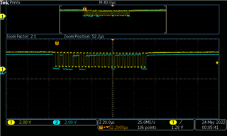
I've attached a screenshot of a scope capture of the I2C signals right at the input pins of one of the 8575 ic's.

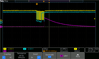
The issue we have is that if I try to set an output high the voltage level is really low, ~125mV. If I set it low, voltage reads 0 from volt meter.

Any suggestions?

  • John,

    Is it possible to share a schematic of your system? It sounds like the outputs are getting pulled down by something if the high and low states are showing some difference, even if it is very small.

    Regards,

    Eric Hackett

  • The "quasi-bidirectional" I/Os of this device have a worst-case IOH of only 30 µA. What is the load?

    Devices like the TCA9535 have stronger outputs, but require more configuration.

    If you set all outputs at once, you could use sixteen '595 shift registers.

  • I removed anything from the output, so open.

  • Hi John,

    Is there a schematic you can share? I'd like to review it and see if everything looks okay.

    -Bobby

  • I should have elaborated a little more, the current schematic isn't the correct. Made some changes to the PCB nut haven't updated the schematic. The FPGA driven SCL and SDA go through a TXS0104 open drain level translator. The 104 is then connected to the PFC8575, there is nothing connected to the 8575 outputs. I'll create a power point of the updated schematic.

  • I'll draw one up and post it tomorrow morning.

  • One other thing, 

    Are you able to put one of the output pins you set high onto the o-scope? I ask because digital multi meters usually use a resistor and read off the voltage drop across the resistor. Since the 8575 has a weak output HIGH state current, you likely may just be reading a low output voltage due to V=I*R where R is large and "I" is at a fixed low output value. 

    -Bobby

  • I captured one of the outputs, screen shot attached. I am thinking that the PCB board designer did something terribly wrong. I am going to look at the power at the IC later this week.

    Channel 3 is P0. As I mentioned yesterday on this particular IC has nothing on the output other than about 1/2" of a PCB trace. 

  • Hey John,

    The scopeshot image on the I2C lines are bit too condensed for me to read but...

    I have a sneaking suspicion I know what may be happening. 

    Could you read off (or take a picture) of the top markings on the device. I suspect, you may have the PCF8575C device which would turn on a fast edge rate after the I2C ACK but then just remain as an open drain output that doesn't drive low so the charge injected from the fast edge rate just leaks out.  (The C version doesn't have a weak output HIGH). I've made this mistake before and saw the same waveform you're showing now.

    -Bobby

  • Yep, it is a C. I will add test this tomorrow with a few outputs tied to VCC. t looks from the data sheet that only 100K is needed on the outputs?

  • Hi John,

    You can add external pull up resistors to have the output state hold a logic high. The value of the pull up resistor should be based on the loading or drive strength you require. 100k pull up is pretty weak but you may be able to use that value depending on what you're trying to drive.

    I wouldn't recommend tying the output directly to Vcc since you could accidently set an output low and have a short from Vcc to GND when driving low. 

    -Bobby