This thread has been locked.

If you have a related question, please click the "Ask a related question" button in the top right corner. The newly created question will be automatically linked to this question.

TCAN1146-Q1: Input Capacitance

Part Number: TCAN1146-Q1


Hello team,

I have some questions regarding TCAN1146-Q1 input capacitance.

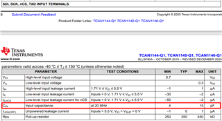
- In the datasheet the input capacitance for TXD is stated as max. 15pF at 20MHz (see below screenshot). Why is 20MHz the test condition?
- What is the input capacitance of TXD at 10MHz or 5MHz, wouldn’t this test condition be closer to application at max. data-rate at 5Mbps?

Thank you,

Muwei Zheng

  • Hi Muwei,

    I believe this test condition is carried over from previous used of a similar SPI block. This would describe why the test condition is outside of the application case for this device as it may be typical for a different device using a modified SPI block. I would expect the measurement results to be similar at a lower frequency more typical for this device's application, as the test frequency is only a sample to conduct this measurement and the actual apartment capacitance will not change much due to frequency. 

    Does the customer have a particular requirement for this specification? Or is this question more on the apparent discrepancy between test condition and expected application conditions? 

    Regards,
    Eric Schott

  • Hi Eric,

    Thank you. We have a follow up question from customer.

    Besides CAN-FD and PN, basically we have strict bit timing requirements, especially for the asymmetry ⊿tBit(Bus). But we could see that we meet the requirements if we can prove Cin of TXD is =<10pf.
    As you know it is a tradeoff between input capacitance and asymmetry timing. Would it be possible to perform a characterization analysis of limited pieces about the application case (e.g. 5MHz) for TXD input capacitance?

  • Hi Muwei,

    The requirement here is regarding the CAN timing symmetry correct? Not SPI?

    The datasheet includes specifications for CAN bit width timings, timing symmetry, and propagation delays. These are all relative to the TXD input with an external load of 0pF, so the pin capacitance is present for these measurements. For this reason, we typically don't specify a capacitance value for this input pin at all, for this device it was simply lumped in to the SPI input pin characteristics. 

    We would not be able to recharacterize this parameter as it would involve a complete test change for the device which is quite the disruptive and lengthy process. Do you think that we can leverage the included timing parameters in the datasheet to show that we can meet the critical requirements on the CAN-side of things? I'm curious how much margin we have on these timing parameters vs their symmetry requirements for example.

    Regards,
    Eric Schott