This thread has been locked.

If you have a related question, please click the "Ask a related question" button in the top right corner. The newly created question will be automatically linked to this question.

Am26ls31cns (transmit) and am26ls32acns (receive) resistance match

Other Parts Discussed in Thread: AM26LS32A, AM26LV32

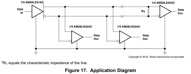
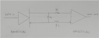
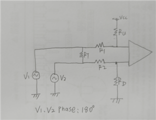
The following two schemes are used for signal transmission. The maximum frequency of the signal is 5KHz and the length of the transmission line is less than 10m.

In order to ensure the integrity of signal transmission and the unknown state will not appear when the transmission line is disconnected.

To know how the following two schemes match resistance, what is the recommended circuit schematic diagram?

① Am26ls31cns (send) and am26ls32acns (accept)

② Am26ls31cns (send) and am26lv32cd (accept)

  • Hi Longchang-san,

    An application diagram is shown in Figure 17 of the AM26LS32A datasheet (shown below). This figure shows a typical layout for a multi-dop receiver setup using these two devices. The termination resistance RT should be placed at the furthest receiver. The value of this termination resistor should match the characteristic impedance of the cable, typically 120-ohms. 

    The AM26LS32A has internal fail-safe biasing. This ensures the receiver remains in a known state if the inputs are left open or disconnected. 

    Let me know if you have any more questions.

    Regards,
    Eric Schott

  • But if the cable is disconnected to the left of the termination resistor, the inputs are not open.

    Only the AM26LV32 has a fail-safe feature for this case.

  • Hi Eric Schott -san

    There are the following circuit applications. What are the functions of R1 and R2

  • Hi Longchang-san,

    These series resistors are typically used as transient protection to limit the fault current through the receiver lines in case of an ESD or surge event. During nominal operation, they do not provide any benefit and in fact slightly attenuate the incoming signal. For this reason, the resistor values are often rather small (~10-ohms) to have minimal impact on the nominal signal case. It's also common to see these resistors rated for relatively high currents as they are expected to survive ESD and surge events to protect the receiver. 

    Regards,
    Eric Schott

  • Hi Eric Schott -san

    There are two additional questions:

    1:On the selection of RT value of terminal resistance

    According to the survey data, the value of RT is usually 120 ohms (according to the characteristic impedance of the cable). Now I have a circuit diagram in my hand, and the value of RT is 220 ohms. I don't know the basis for selecting 220 ohms; I would like to ask whether there is a design case where the terminal resistance rt=220 ohms, and what is the consideration point for selecting 220 ohms?

    2:Broken line fault protection

    ①For the receiver with fault protection, if the external pull-up resistance(R3,R4) is added, what will be the impact on the receiver?

    ②How to select the resistance value of external pull-up resistance(R3,R4) for receivers without fault protection?

  • Hi Longchang-san,

    1. The primary purpose of termination resistors are to ensure the signal line network does not end in a high impedance terminal. Leaving out this resistor would cause signal energy to reflect off of the unterminated end-point and causing ringing in the bus. This can impact signal integrity and limit the achievable data rate on a network. 
    To most effectively dampen these signal reflections, the value of the termination resistor should match the characteristic impedance of the cable. However, if this is not possible or desired, including any comparable value of Rt will still help reduce network ringing. In this case, the value of 220Ω may have been chosen to reduce BOM variance or to accommodate for a variety of cable possibilities. It may also simply be a typo where a 120Ω was intended. It's also common to see larger Rt values where partial termination is used in multi-drop applications - but this is likely not the case given the devices being discussed here. 

    2. The external biasing resistors R3 and R4 will form a "fail-safe biasing circuit" for the network. The goal of this circuit is to keep the differential in a known state when the network's driver is in a high impedance state. The app note linked below goes into detail on how to calculate these resistor values and what impacts such a circuit has an a network. Let me know if you have questions on this document. 
    https://www.ti.com/lit/an/slyt324/slyt324.pdf 

    Regards,
    Eric Schott

  • Hi Eric Schott -san

    As for the chip with wire break fault protection function, the function of adding pull-up resistance externally can be understood as adding pull-down resistance externally to the chip to make the wire break fault protection function of the chip more stable?

    Considerations

    The chip has broken wire fault protection. When connected with external circuits (the value of the pull-up resistance integrated in the chip is changed), the broken wire fault protection is unstable. In order to make the function of the broken wire fault protection more stable, the pull-down resistance with appropriate resistance value is artificially added outside the chip during circuit design.


  • Hi Eric Schott -san

    Additional questions

    In order to ensure the reliability of RS422 communication, must the pull-up resistance be added

  • Hi Longchang-san,

    When an RS422 node is disconnected from an active driver, the bus is floating. Due to various leakage paths, the A and B signal line will become equal in this state, so the differential voltage Vdiff is near 0V. The RS422 electrical standard defines the input thresholds for the differential receivers: above +200mV is considered a logic high, and below -200mV is considered a logic low. Any differential voltage where -200mV < Vdiff < +200mV is undefined. The disconnected state allows the differential to be in this undefined state which is undesirable. 

    External fail-safe biasing resistors can be added to the A and B lines to bias the Vdiff outside of this undefined range when they are disconnected from an active driver. This means that the RS422 receiver output will remain in a known state in the case of disconnection or break fault. Some transceiver will include internal fail-safe biasing in order to preserve this known receiver state when the A and B pins are open. 

    During normal operation, there is an active RS422 driver on the bus that strongly pulls the A and B lines to their desired voltage. During this state, the driver is capable of keeping Vdiff outside of the undefined region. The external fail-safe resistors should ideally have no impact on the system when it is operating in this way. Therefore, it is important to value the fail-safe resistors so that they are weak enough to not impact normal operation, but strong enough to reliably bias the bus state in the case of a open or break fault condition. 

    Regards,
    Eric Schott

  • Hi Eric Schott -san

    Transceiver with include internal fail-safe,If the pull-up resistance is added externally,

    What is the function of resistance And how to evaluate the resistance value of the resistance?

  • Hi Eric Schott -san

    Additional questions

    The application notes in the following links only explain the calculation of the pull-up resistance when there is no signal source on the AB line.

    If there is a signal source on the AB line, how to calculate the pull-up resistance value?

    https://www.ti.com/lit/an/slyt324/slyt324.pdf 

  • It is assumed that the transmitter is strong enough to pull the lines in the opposite direction. (If the pull-up/-down resistors are much weaker than the termination resistor, this is obviously the case.)