This thread has been locked.

If you have a related question, please click the "Ask a related question" button in the top right corner. The newly created question will be automatically linked to this question.

TPS65988EVM: TPS65988EVM

Part Number: TPS65988EVM

Hi,

I am designing a custom board to source power using USB C ports to two sink devices and I am very close to finishing my design. I need the following information if someone can provide me

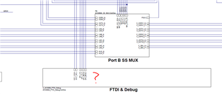
  1. What is the function of the FTDI circuit on the EVM board? ( To communicate with GUI to upload configuration?)
  2. Is there some OTS FTDI board available that I can use for custom PCB to save space? What should I consider while choosing the FTDI board? 
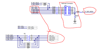
    Following are the FTDI connection with the rest of the circuit on EVM

    FTDI BOARD CONNECTIONS

    1. SPI MISO
    2. SPI CLK
    3. SPI MOSI
    4. SPI CS
    5. I2C1_SCL
    6. I2C1_SDA
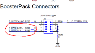
  3. What is the function of DEBUG header pins on the EVM board? Do I really need them at any stage for programming or configuring?
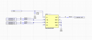
  4. What is the function of the Current Sense Circuit?
  5. Can I configure TPS65988 with Aardvark instead of FTDI?

https://ftdichip.com/product-category/products/

  • Hi,

    Our team member will get back to you as soon as possible.

    Regards.

  • Thanks for an update

  • Hi Ali,

    Yes, you can configure the TPS65988 with Aardvark instead of FTDI. To answer your question about the current sense circuit, it exists to monitor the current flow for functions such as overcurrent protection. 

    Since Aardvark can be used, would you still like more information regarding your questions about FTDI?

  • Hi
    Thanks for your reply. Can you help me to define the pinout for Aardvark? Will it be I2C1 OR I2C2 will use for it? As in TPS25750, master I2C is used to configure the settings for it. What will be the case for TPS65988EVM? I will also still keep the option for FTDI pinout on board so If I need to communicate with FTDI, I can do it.
    Can you also provide me with some documents which explain the procedure for configuration using GUI? TPS25750 has everything in detail in its EVM Guidelines but I couldn't find it for TPS65988EVM. On FTDI  schematic page, there is also EEPROM. Do I need any EEPROM in the case of Aardvark? In TPS25750, we flash the configuration to EEPROM but I don't know how we will save our configuration in TPS65988EVM. If we need it then can you help me to define its connection with TPS65988?

    Last, if you can elaborate on the function of Debug header pins. I don't have space to place header pins for all those pins or connections. So Can you help me define the pins which may need me during PCB configuration for TPS65988?
    I will wait for your valuable feedback. Thanks

  • Ali,

    Please give us some time to answer all your questions

  • Sure,
    I will wait for your further instructions

  • Hi Ali,

    I will address your questions in order below:

    1.) The pinout for the Aardvark connector matches the Aardvark (J10 header) pinout defined on the TPS65988EVM User Guide (page 21). If you wish to use the Aardvark to communicate with the PD controller, you can use I2C1 or I2C2. If you wish to use the Aardvark to program the PD controller, then you will have to use SPI since the FLASH is connected via SPI. Those choices are up to you and your design parameters.

    2.) TI has application notes, video tutorials, and other content on the TPS65988 webpage that could be useful in explaining the GUI configuration procedure. You can find this webpage at https://www.ti.com/product/TPS65988 

    Programming the EVM using Aardvark also requires the use of FLASH to store and load the configuration to the TPS65988. You can look at the TPS65988 datasheet SPI controller interface section (section 8.3.13) for more details on SPI FLASH communication.

    3.) The debug header can be used for purposes such as addressing an unestablished connection or abnormal resetting behavior. In the EVM schematic, the debug header is labeled J8. If you are extremely short on space, fitting headers to just the I2C or SPI connections should be sufficient.

    Thanks

  • Hi 
    Thanks for your great feedback.
    1: I will place this connector on the PCB but will change the netlabels of course because it is for FTDI and I need to flash using Aardvark.

    2: I couldn't understand the connection of J8 with TPS65988. FTDI schematic even does not have any port related to SWD-CLK and SWD-DATA.

    So how it will communicate with TPS65988?

  • Hi Ali,

    I am looking into the debug connections and will get back to you shortly.

    Thanks

  • Hi Ali,

    I misspoke before regarding the purpose of the J8 header. The J8 header labeled "debug" does not contain I2C or SPI connections you would need, it was for legacy internal use. The Aardvark connector will allow you to debug the I2C and SPI connections using the GUI tool (same as if you were to use FTDI/TIVA). If you are looking for connections apart from that, the J3 and J4 headers contain I2C and SPI connections that can be used. However, using the Aardvark connector should be sufficient.

    Thanks

  • Hi 
    Thanks again.
    I think I am all settled with this query.
    I will add a connector with the following netlabels. It has I2C and SPI connection that is a J10 connector in EVM.

    1. SPI MISO
    2. SPI CLK
    3. SPI MOSI
    4. SPI CS
    5. I2C1_SCL
    6. I2C1_SDA

    I also have some other questions. I think I should create a new thread because it is about ADCINX pins which I believe are redundant in my case with a dip switch and different voltage divider.
    Thanks for all your help.

  • No problem.

    Thanks