This thread has been locked.

If you have a related question, please click the "Ask a related question" button in the top right corner. The newly created question will be automatically linked to this question.

DS90UB935-Q1: DS90UB935TRHBRQ1 Schematic review

Part Number: DS90UB935-Q1

Hi Team,

There is a good new that we DIN DS90UB935TRHBRQ1!!!

And still need your support to make sure DWIN DS90UB935TRHBRQ1 , THX

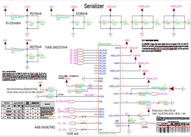
Please refer to attachment for the clearer SCH,

1. Does the module peripheral circuit design meet the DS90UB935TRHBRQ1 requirements?
2. The POC recommendation of 935 is shown in the schematic sheet. It may be possible to use two levels to meet the requirements. Please provide the corresponding test data. Does this project meet the requirements with three levels?
3. Do the power supplies VDDD, VDDPLL and VDDDDRV have to be connected with magnetic beads?
4. What is the voltage of pin12 (LPF2)? Is it sufficient to use a 6.3V withstand voltage capacitor?
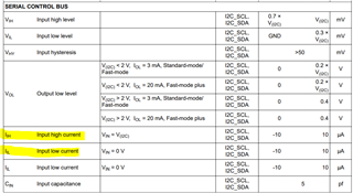
5. SCL and SDA are open-drain state, what is the actual internal resistance? How much current sink capability does it have? Does the pull-up 1.5K meet the requirements?
6. The ESD test on the coaxial pin was not prevented from causing damage. A reserved ESD device was added on pin14 (Dout+). The parameters of the ESD device are as follows. Does it affect the signal? Or what parameters need to be met to use?

DS90UB935TRHBRQ1模块原理图设计审查单V1.0_20220611.xlsx

  • Hello Kygo,

    1. I can review the schematic in more detail and respond with comments within ~1 week.
    2. For the 935/936 parts, we recommend using 3 Ferrite Beads for the PoC network on both boards with the exact components listed in the datasheet, in order to avoid any issues with the link quality. If different components are used, then customer would need to verify that the PoC network maintains >= 2-kOhms impedance over the frequency band of the channel link and does not significantly impact the channel link quality. Also need to verify that less than 150mA of current is going through the selected PoC network. I will look for relevant test data, but typically the 3 Ferrite Bead solution is recommended. We also do have alternative designs, but those are under NDA.
    3. We do require Ferrite Beads at the VDD power supply pins, as specified in the datasheet's Typical Applications diagram. The Ferrite Bead is to ensure a stable 1.8V(+/-5%) is present on the VDDD, VDDPLL, and VDDDRV after pulling HIGH. The current version of the datasheet has a small typo, so the Ferrite Beads used on these pins should have Z=1-kOhms@100MHz and DCR<=500-mOhms. Depending on the noise in the customer's voltage rails, more or less capacitors may be added in order to meet this requirement, but that is a system-level discussion that would probably need simulation in customer-specific systems. For now, I recommend following the description in the Pin Functions table in the datasheet and follow the Typical Applications example in the datasheet as well.
    4. It is sufficient to use a 6.3V capacitor at the LPF2 pin. For reference, our 953 EVM uses p/n C0603X5R0J104K030BC at the LPF2 pin.
    5. Sink current is defined in the 935 device datasheet:
      1. General recommendation for I2C pull-ups is a value between 470-Ohms to 4.7-kOhms, but the optimal pull-up value depends on the I2C data rate on the bus and the I2C bus capacitance on the actual PCB board. We have an App Note that can help calculate the optimal pull-up on the I2C lanes, based on those values, which is linked below:
      2. https://www.ti.com/lit/an/slva689/slva689.pdf?ts=1655145555483 
    6. Our FPD-Link devices already have built-in ESD protection, without needing external ESD diodes. See the ESD Ratings table in the device datasheet for more details. External ESD diodes are not needed in order to prevent link loss, high bit errors, etc... They are only used to prevent device damage. As long as layout is performed well (50-Ohms(+/-10%) single-ended impedance, minimal parasitic capacitance, etc...) and the S-Parameter channel requirements are met for the devices used, then external ESD diodes are not needed. 
      1. If external ESD diode is used for the 935 device, then make sure the capacitance is about <0.5pF. But depending on some systems, the capacitance might need to be lower.
      2. Since ESD diode is placed behind the AC coupling capacitor, on the pin side, then you do not need to worry about the standoff voltage rating of the diode.
      3. Our systems are validated with the ESD diode on the other side of the AC coupling capacitor, closer to the connector. Customer would need to simulate S-Parameter performance of the channel link if ESD diode is placed on the other side of the AC coupling capacitor, to make sure there are no SI issues.
      4. A brief overview of ESD diodes is given in this App Note:
      5. https://www.ti.com/lit/an/slvaf60a/slvaf60a.pdf

    Best,

    Justin Phan

  • Hello Kygo,

    Here are my comments on the schematic:

    1. If cost reduction is a focus, then I recommend using the Synchronous Mode setting on the MODE pin. If the connected deserializer is a CSI-2 part, such as the 936, 954, 960, etc... then you can use the reference clock on the deserializer board as the reference clock for the 935 as well. The reference clock signal gets sent over the Back Channel (DES->SER). You can save cost, since you do not need an oscillator on the CLKIN pin of the 935 in Synchronous Mode. This Mode will not work if paired with the 914A or 933 deserializer devices.
    2. The PDB connection is not shown in the schematic. If a separate SoC is controlling when PDB pulls HIGH, then make sure that the Power-Up Sequence defined in the datasheet is strictly followed in the customer system. If a separate SoC is not used, then make sure an RX circuit with 10-kOhms pull-up and >=10uF capacitance is used, in order to delay when PDB pulls HIGH, as demonstrated in the 935 datasheet's Typical Applications figure.
    3. Optimal pull-up resistors on the I2C lines depends on the desired I2C data rate and the bus capacitance of the I2C bus on the PCB. Recommend using App Note SLVA689 to calculate the optimal pull-up resistors in specific customer systems.
    4. The Ferrite Bead used on the VDDD, VDDDRV, and VDDPLL pins is BLM15BD102SZ1, which has Z=1-kOhms@100MHz and DCR=900-mOhms. The DCR is too high and may cause significant voltage drop across the Ferrite Bead, which may cause datasheet specs to be violated. We actually recommend a Ferrite Bead with a DCR less than 500-mOhms. For reference, our 953 EVM uses BLM18AG102SN1D. Recommend to use the same or similar part.
    5. ESD diodes are most effective when placed near the ESD source, such as the connector, so that it can shunt more energy away from the device. If placed near connector, will need to be rated with enough standoff voltage in order to not be triggered by PoC voltage.
    6. ESD diodes and any other extra component along the channel link will typically degrade the signal quality. We recommend minimizing the number of extra components along the high-speed signal traces.
    7. If ESD diode is placed behind the AC coupling capacitor (on the device side), then recommend customer to use simulation and physical measurements in order to make sure the ESD diode does not significantly affect the signal quality and that good channel parameters are still met (Return Loss and Insertion Loss).
    8. Our FPD-Link devices already have internal ESD protection, so the use of an external ESD diode is not required. See the ESD Ratings table in the 935 datasheet for the specific ESD ratings on the device.
    9. We currently do not have test data that directly compares the performance of using two Ferrite Beads vs three Ferrite Beads in the recommended "4G" PoC network. listed in the 936 datasheet The decision to use two or three Ferrite Beads is a system level decision. The goal is for the PoC network to maintain greater than 1-kOhms impedance over the operating frequency range of the channel link (Back Channel frequency to Forward Channel frequency). Ferrite bead impedance characteristics are affected by the current that runs through them. If the customer is using a low-current application that draws about 50mA of current through the PoC network, then it may be possible to use two Ferrite Beads in the PoC design. However, if the current goes above 100mA, then three Ferrite Beads will be needed. We generally recommend using three Ferrite Beads in all applications of the "4G" PoC network, in order to guarantee that the PoC network will not negatively affect the channel's signal quality. The PoC design in the datasheet is only rated up to 150mA. But in any case, we recommend customer use simulation and physical S-Parameter measurements in order to verify that the chosen PoC design will not have a significant impact on the channel's quality in the customer system.
    10.  I also noticed that the inductor and resistor used in the PoC network schematic do not match what is used in the 935 datasheet. If customer is using different components than what is listed in the datasheet, then they will need to be responsible for validating that their custom PoC network will not negatively affect the channel quality in the customer system. 
    11. Recommendation is to use the exact same "4G" PoC network listed in the 953 datasheet and to use the exact same or similar components listed in the datasheet as well. The "4G" PoC network in the datasheet is only rated up to 150mA, so make sure the current through the PoC network is less than 150mA.
    12. Additional PoC networks with different ratings can be provided, under NDA.

    Best,

    Justin Phan