This thread has been locked.

If you have a related question, please click the "Ask a related question" button in the top right corner. The newly created question will be automatically linked to this question.

THVD8000: Railway conducted noise immunity : 150kHz-80MHz, 10Vrms 80% AM 1kHz FAILS

Part Number: THVD8000
Other Parts Discussed in Thread: THVD8010

Hi team, 

I have been doing some measurements for pre-compliance of railway norm (0Vrms conducted noise with 80% AM at 1kHz, from 150kHz to 80MHz) and ... I don't manage to pass : the Amplitude Modulation at 1kHz looks like a 1kHz OOK modulation for the THVD8000.

There are some problems with my setup and I know it but not everything can be as perfect as we hope (even in the final implementation in the train) :

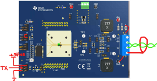
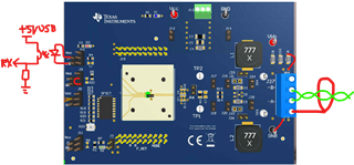
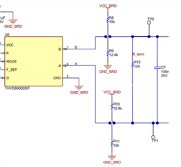
I'm using 2* THVD8000 evaluation modules, one with a USB-uart adapter with the THVD configured as always TX, the 5V USB power powering the local board and the 10m away board through the PLC components, then a 10m cable loop, another EVM configured as always RX and returning data over optocoupler to the initial USB-UART adapter (both EVM as taped back to back (20mm away from each other).

The 10Vrms conducted is done on the shielded cable (didn't have a 120Ohm railway compliant cable as it will be in the train laying around so I'm using a normal shielded 0.75mm² cable)

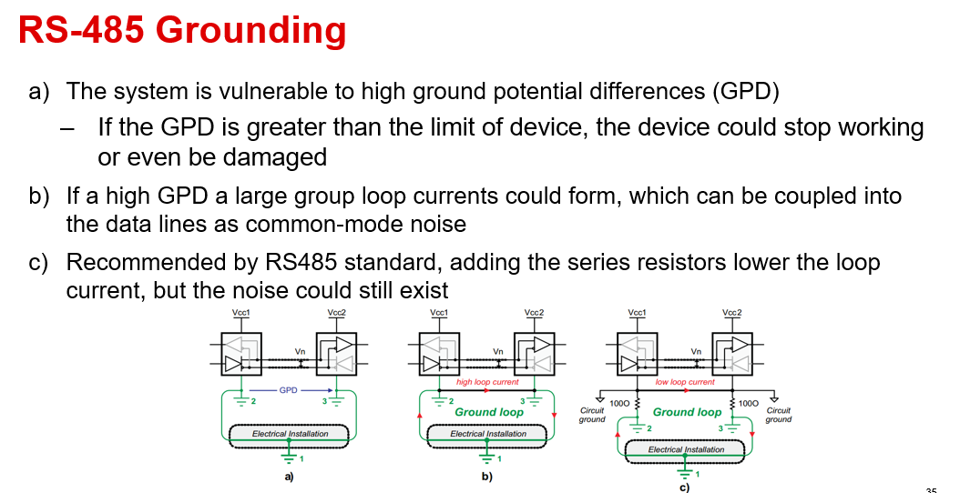
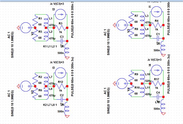
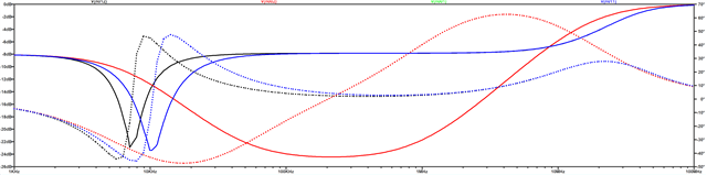
The EVM are set for 5MHz modulation and common mode noise translates to differential somehow (pickup coils that are +/-20% variation?) at around 5 & 10MHz (+/-20% around those fundamental and first harmonic)

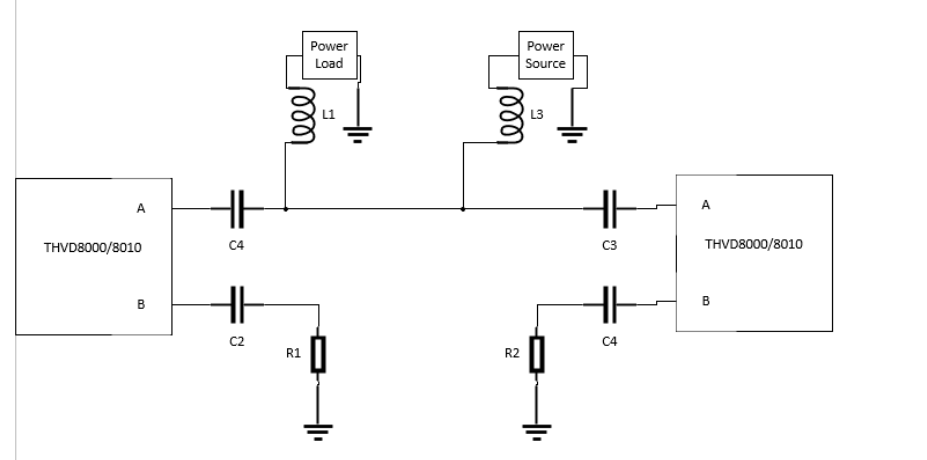
I tested replacing the L-C extraction/injection by a PoE transformer (wurth split primary) but I got info from them that if used with DC current (with differential current, not common mode) the transformer saturates, and from my measurements it's even worse for common mode noise immunity than L-C.

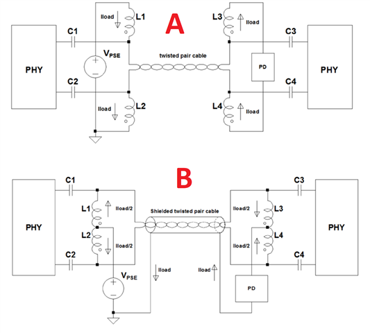
I've yet to test a power choke dual coil (to have better matching between inductors = less common to differential noise translation) and to use the cable shield as negative conductor (see page 3 of https://www.ieee802.org/3/cg/public/Sept2017/stewart_01_0917.pdf)

Thanks for your suggestions, help, ect.

  • Hi Alexandre,

    Thanks for reaching out!

    What standard are you testing the THVD8000 to with respect to conducted emissions ?

    What is the power source (not IC power - but bus power that goes through the inductors on the EVM) voltage?


    Where are you measuring the conducted emissions at? 

    To verify what is the characteristic impedance of the cable you have been testing with? I see a few variants online with the parameters given and I want to understand what you are using?

    So with all those questions out of the way - there are a few possibilities to what I think could be problematic:

    1. What is the capacitance on the bus power source - is there any bulk capacitance? Also I am pretty sure its DC based on the question -- but could you verify? So ultimately one thing that is assumed in the THVD8000 design is that the inductors are connected to "AC ground" (this is relative because the power source can be AC but it needs to be decades lower in frequency for proper operation) - that AC ground is created with the assumed bulk capacitance at the bus power source/load. I ask because I have seen issues with noise after the inductor that basically was the THVD8000 signal - and this was due to the node not being close enough to an "AC ground" for the filtering to take place. 

    2. Using closer matched inductors (the 20% variation could possibly cause issues) isn't a bad move to test to see if it helps - I still think it may have to do with point 1 - but this doesn't seem like a bad idea. However Its not a issue that we typically see (inductors used in a lot of these applications have wide tolerances), but it could be a partial contributing factor.

    3. While I don't think this is the main problem - adding a common mode choke (with low series resistance and low differential inductance) can help clean up any common mode noise that may be picked up by the long wires of the applications and as long as the added series impedance is low it shouldn't have a major negative effect on device operation. 

    Ultimately it does seem like there is noise from the system due to something not being properly filtered based on the information that I have right now. The THVD8000 does have Spread Spectrum Clocking which will cause deviations in the modulation frequency so the deviation you see in the noise form is likely just due to that. Please let me know if you can answer the questions I have asked above and I will see if there any more nuanced advise I can give you - I do have a decent feeling it has to do with the THVD8000 not "seeing" an AC ground after the inductor however. 

    Please let me know!

    Best,

    Parker Dodson

  • Hi Parker,

    The standard is NEN-EN 50121-3-2:2017 which points to basic standard EN 61000–4–6 for the radio frequency common mode noise.

    Currently the power source is the 5V USB, but later it will be 24V rail with DCDC converters on each end to power the ICs with 3.3V.

    not emissions, immunity

    I'll try to measure the impedance of the cable I'm using. currently it's a FILOTEX EN50306-4 3P 300V 2*0.75mm² + Shield, I can't find back the ordering code... but it's not a controlled impedance cable. just a single twisted pair cable with shield.

    I've set my EVM like this with a USB-serial TTL converter, shield is connected to ground, not sure it's the best :

    1- not sure to understand, but maybe the above drawing helps

    2- I'll try this week with dual coil inductors and common mode chokes (with shield as negative wire)

  • Hi Alexandre,

    I apologize - I misspoke with the emissions versus immunity. Thank you for the reference standard.

    We don't typically look at conducted immunity so we don't have a ton of data on that. If possible can you show a diagram of where you are injecting and measuring the noise signal for the test setup - I am a bit confused with your setup versus the standard and I just want to ensure I am understanding your setup completely. I see the diagram you attached before and that is helpful for the THVD8000 setup but I want to fully understand the setup to make sure I understand where noise is being injected and where it is being measured because I am reading this as like you are injecting the noise signal onto the "D" pin of the device and measuring the noise at the cable, I could be wrong and just misreading it, but that's why I want to clarify to mitigate any misunderstandings. I apologize for the inconvenience - but I just want to ensure I understand where noise is injected and where it is measured again (I believe its being measured on the cable - but I want to double check) 

    To clarify - are you planning on moving power and data over the transmission line - as in the 24V signal will be on the line with data (and DCDC converters will step that down at IC side) ? I ask because the diagram you sent doesn't show you testing with the power source loads (if they will be there at the end equipment) - if these are too be included in the system I would highly advise running tests with those systems attached as it could affect the results of the test - also the power coupling would be floating in this test case which could cause issues (if using the EVM - they are L1 and L2). Does the standard not want you to include the other devices on the bus? 

    As mentioned above the main things you can do to the system that I have seen with respect to common mode noise immunity (while we don't spec it directly we do see requests still) and adding a common mode choke could help reduce the common mode noise on the bus- ideally the twisted cabling would have some effect here but it may not be enough. If you find some success or issues with this approach in your further testing please let me know so I can see where we could be standing at. 

    Please let me know 

    Best,

    Parker Dodson

  • Hi Parker,

    I'm injecting with an CDN EMclamp (1m long device that receives the RF signal from the generator, see below picture) placed 20cm away from the receiver EVM on the shielded bus cable (cable shield is directly connected to both EVMs ground plane), the clamp sends noise on one side (last 2 sections, and absorbs on the other side (to protect Associated Equipment, so that only the DUT is tested). This clamp and this level (10V/m) are calibrated and follow the standard EN 61000–4–6 test method and amplitude (and our equipment is calibrated to perform this).

    What is being measured is the data coming out of the receiver EVM, on the PC, after translation by the serial TTL-USB translator, I checked on the output of the THVD, the noise is not picked after the THVD, it is the THVD 'decoding' it from the bus pair. When noise is forced on the cable shield, and without sending data from the emitter EVM, the receiver THVD still sees data due to the AM modulation of the conducted noise (and I think it happens because common mode noise is translated to differential)

    I forgot to explain my diagram, on the bus connector there is a VCC-GND of the transceiver, and on North and South of the connector there are vias of VCC-GND and further North and south there is the outputs of the inductors GNB and VBB, so I made a jumper between those : 

    - on Emitter EVM, the USB power goes to THVD, then to connector vias and is injected on the bus cable

    - on Receiver EVM, the Bus cable power is extracted and connected to THVD power.

    So currently everything runs on 4.5V, but final application will be 3.3V THVD and 24V bus voltages, the DCDCs from battery and for 3.3V will be designed to have very little impact on noise so I'm ignoring them for now.

    In the final application I'll also have different inductors for injection because I need to have lower effect from the max 25 devices on the bus. (15 max is also fine for the current project).

    I know my use case is a bit harsher environment than the THVD8000 was probably designed for and I also have a lot of imperfect test conditions (cable is not 120Ohm, inductors will still change, etc.) but I hope to get some testing ideas.

    I also got the information that using the shield as negative wire and the bus (P+N) as positive wire could make it possible to extract power with a single common mode choke instead of a power choke (as the core doesn't support the full DC bias), that's what I point out at the end of my initial post :

    and because the capacitors have the same bias also have the same capacitance and impedance so less common to differential mode conversion.

    Please give me your thoughts if it's a good/bad idea. Is it okay for the cable shield to share ground with the THVD (in both cases) ?

    Regards, Alexandre

  • Hi Alexandre,

    Thank you for the details that you have shared - I really appreciate the detail!

    Before I go into your response - one thing I did want to note - is that if you don't need the 5MHz modulation frequency and can shrink it down to 300KHz the THVD8010 is essentially a slower but more robust version of the THVD8000. If you need the higher modulation because you have higher data-rate requirements the THVD8000 is still probably the best choice - I just wanted to let you know that we do have a THVD80x0 device that was designed with more harsh environments in mind. 

    I think I understand the full scope of the issue you are having now so a few comments are below:

    1. For the power choke/common mode choke diagram that you have shown I will say a couple things. The above image is what we push for the design on THVD80x0 devices - that is the common implementation. However the second implementation isn't one that we typically  push - for power sources/ power loads that are set up in that manner - we typically have a pseudo differential setup - where the THVD80x0 is operated more or less as a single ended device (shown below - termination not shown but still can still be used):

    Where the cable grounding and the THVD80x0 grounding could be the same ground plane - there is some nuance here because chassis/earth connections and signal ground connections also typically coexist in these types of applications - a little more on that in a bit.

    However - the implementation that you show could potentially work - typically we just don't see it as the reason customers typically tend to go towards the diagram I show above and not the second diagram in what you added is that you half the amount of inductors on the bus (at the cost of some distance as the driver magnitude is slightly diminished in this use case). The one thing that I would be concerned with is high loop current - as this is a known phenomena with RS-485 transceivers that they are susceptible to common mode noise due to high ground loop current. If in this application there is a "chassis" or "earth" connection the loop current can be diminished as shown below:

    If this is not possible - there still could be improvement due to the ability of a common mode choke (since the power chokes core will be saturated in this application from my  understanding) but I just wanted to add that there is a potential for common mode noise in this use case and we do have a suggested work-around if it is able to fit your system. 

    As far the communication of the bus is concerned - this is basically the same implementation - the power loads/sources should be seen as AC grounds so that essentially the THVD8000 doesn't see anything past the inductor connection on the bus - since it is DC thats pretty safe assumption due to bulk capacitances typically found around the DC -DC converters (many applications the load and source are just DC-DC converters) so I don't see a major issues there - only with the potential common mode noise due to higher ground loop current - but it may be still prove to be less.

    Finally one thing that I want to add - is we do have a "EMC" immune RS-485 guide -its specific to one use case but the information in it can be generally applied to many RS-485 applications. https://www.ti.com/lit/ug/tidudf5/tidudf5.pdf?ts=1655320292600 section 2.2.1.1.2 on page 7 it goes through a few alternatives to adding common noise immunity to the circuit. Essentially beyond what has been talked about already it includes a split termination (the terminating resistor is split with a capacitor to ground on the mid-way point), filter caps to ground on A or B (this is a bit tricky with the THVD80x0 as these impedances from the capacitors must be taken into consideration  when designing the inductor values of your system), and/or series pulse resistors that can help block some of the transient noise. One thing to note about this design is it doesn't spec to 61000-4-6 but it does for IEC 61000-4-2/-3/-5.

    So while not a perfect solution it does have some content that can help improve performance in other non-tested standards as a lot of this document still resolves around common mode noise (which the RS-485 portion is tested against - just not in the same fashion as described in 61000-4-6) 

    I think the ideas that you have so far are good options to pursue because they definitely seem like they could be possible and potentially provide more system level benefit than the current implementation.

    Please let me know if these solutions are possible to try from your side - and if you are able to test them and have new result data I'd love to see so if we need to adjust any of my  recommendations to tackle more specific problems - but I think the ideas so far are probably a good starting point in helping increase the common mode immunity of the design.

    Best,

    Parker Dodson

  • Hi Parker,

    I actually have another question related to THVD8010 & the THVD8000 EVM resistor dividers at the input of the THVD, are they for adding offset to improving immunity to noise or something else ? (the resistor dividers are not placed by default, the 100nF caps neither because I can't filter on each device if I have 15-25 nodes)

    then answering your questions : 

    I could move to 300kHz but with 15-25 nodes the inductance required on each node is a bit crazy (3-5mH !)

    Pseudo-differential in my case is a bad idea I think (because of the crazy common mode noise), and you still need an real inductor (big) that carries the DC current in it's core flux, with a common mode choke (dual inductor on the figure) it can be as small as a 1206 common mode choke and be 1mH because the core is not gapped and can't carry DC current, but using the shield for current return means no DC current flux on the dual choke.

    Shield aka ground was planned to be capacitively coupled to the housing = chassis of the train because I'll switch the shield=GND to connect the devices to the bus one by one in series, to be able to detect them in the order they are on the bus, so I can't have chassis shorting the shield, I can add a series resistor to it to calm down the chassis loop though.

    Yes I didn't test yet against EFT (EN61000-4-2/-3/-5), that's another problem later.

    Center point termination is already present on the transmitter side (as it will be present internally) but the termination on the receiver 120Ohm only is doable but not easy to have center termination (it would require a PCB on the mating connector of the last device)

  • Hi Alexandre,

    The resistors (R8,R9,R10, and R11) on the EVM (when placed) are used to set a known voltage between A and B (~310mV for 3.3V and ~475mV for 5V) this allows the receiver to detect a valid logic condition on the bus in cases of Open and Idle bus + margin for noise  as the thresholds are lower than what the idle voltage would be set to. Also as a note on the capacitor - it is there to help simulate a long  cable and not necessarily a suggested terminating capacitance - the value isn't super set in stone and is there to help get a rough estimate of how different cable properties and lengths could affect the output drive strength. 

    Understandable - the large inductance values for lower frequency systems are not desirable in a lot of applications. There are work-arounds - but they aren't necessarily simple as it would require a line-driver to be able to lower the minimum impedance that the system could drive or remove all terminations to lower the min impedance from A or B to ground to 60 instead of 375 - but it most likely wouldn't be beneficial for noise in the system. 

    I agree the pseudo-differential is not the best for this system - it was more of reference of known designs - but I think the implementation that you have suggested (with the added series resistance to help lower loop current - since in your system the recommended solution isn't practical) is probably the best approach. 

    On a note on the terminating capacitance - I understand that is going to be difficult - but if the proposed next step (ground sharing essentially) does not prove fruitful enough that is the next step I would take - however I do think the original proposal should improve the system quite a bit even just with some series resistance - the large common mode range of RS-485 should help in this regard. Filter caps to ground from A or B or a cap between A and B may prove to be pretty useless due  the amount of nodes in your system and the impedance to ground budget you will have for each line - so understandably not a great approach. 

    With all that being said - 

    Do you have any lingering questions before you attempt the testing with the new grounding scheme + common mode choke that I may be able to help resolve? 

    If not - and the tests show negative results - please let me know and if possible share an overview of the new results and I can take a look to see what other areas could possibly need to be tweaked.

    Best,

    Parker Dodson

  • Hi Parker,

    I've done some tests with a dual power choke of ~1mH each coil (470uH when in parallel on the bus) with power on A/B lines, not using shield for power.

    Currently the 10V/m common mode noise at 10MHz (with 5Mhz OOK config) is ~300mV, so I need the THVD8010 threshold VMAG_ONE & VMAG_ZERO (<0.3V & >1.2V), is it possible to simulate that with the external PU & PD resistors connected to the rails to the A/B lines ? (external resistor of the EVM I was speaking of last time)

    Thanks for your help.

  • Hi Alexandre,

    So the resistors are really there to help idle bus noise margin - not an active bus as much. Adding a 300mV - 400mV (so like 1.5/1.6 on A and 1.2 on B for example) bias between A and B may help prevent glitches and it might be worthwhile to try since it would be simpler than the THVD8010 - but I don't think you will get the same robustness out of the THVD8000 and my biggest worry is the bias may prevent the THVD8000 from properly detecting "low magnitude" state since the thresholds are much tighter. However adding a few test resistors is probably less of a hassle than looking at the THVD8010 - and with only 300mV of noise I do think it would worth while to try - because as long as the impedance from B to ground and A to ground is much lower than the bias resistors it may not be an issue on the 'low magnitude detection'

    Please let me know if you have any other questions and if you have any results form the pu/pd resistors!

    Best,

    Parker Dodson

  • Hi Parker,

    I forgot to mention but I do have a few THVD8010 just in case, but inductors would need to be huge or termination resistors removed for PLC type A (see above edited diagrams.

    I've done a lot more tests and there were multiple layers of discoveries :

    1- I've measured with a Bode 100 (frequency sweep RLC measurement) the inductors, coupled inductors and common mode chokes (for PLC type B) and all have serious SRF limitations, meaning there is no use in going as high as 5MHz OOK, because all components have worse impedance at those frequencies (parasitic caps are more serious and inductors are already capacitive), so 500kHz-2MHz is my best bet. so I started thinking more about using 1MHz after this. I also measured Common mode chokes saturation (use in PLC type A) and I must forget trying to use them, they loose all inductance in the first 5% of their common mode current rating, but I could use them in the PLC type B, which I tested later.

    2- Testing for high common mode noise (10V/m) at 1-50MHz (worse range) I noticed that higher baud rate doesn't seem to be more susceptible to noise than lower baud rate, but obviously the lower the easier it is to oversample and clear glitches, I used up to 56kbaud (max the optocoupler setup RX signal accepts)

    3- Same thing for different OOK frequencies, 1MHz setup is less sensitive to pickup noise than 5MHz, so I used that instead.

    4- Comparing test results with the emitter grounded instead of the receiver, I concluded that the latter is worse and as all devices need to receive at some point I only tested with the received after. At some point I concluded that grounding the receiver was worse than having the bus grounded through the PC USB port, but I discovered later than somehow that AIO PC in our lab has USB ports & housing floating towards the 220VAC plug earth pin.

    5- having a hard grounded shielded cable common to the IC ground seems to be better than to try to isolate the receiver from the noise coming from the cable shield. Capacitive or ferrite between chassis/shield and IC ground has worse behavior (more fake characters received) and because it's similar to RS485 grounding technique C (although I didn't use a 100Ohm resistor but ferrite), RS 485 grounding technique B will be used, I'll leave a 100Ohm resistor possibility on nodes (not possible on controller with PLC type B because of the type of connector used).

    6- I tested PLC type A & B with split coils and it's not worse against 10V/m conducted RF immunity test as I expected it was : because inductance is +/-20% so common mode could translate to differential mode but the impedance is already quite high so apparently not a problem. 

    I wonder if using a coupled inductor (or a common mode choke in PLC type B) would actually help reduce common mode noise or create some differential mode (because the "center tap" of the coupled inductors is AC connected to ground and noise is relative to ground too), do you know how to simulate this accurately ?

    I create this where and the result seems to be that a coupled inductor/choke in the correct orientation (top left) actually absorbs some of the common mode noise (red line is one of the bus traces). If I create imbalance (+/-20% on bottom right split inductors) then I can simulate common to diff noise transfer...

    ltspice file attached

  • Hi Alexandre,

    Thank you for the detailed update!

    I agree with the conclusions you've made so far based off the results that you are seeing

    For the simulation:

    If you have a .lib file or some base spice model you can zip it up and drag the zipped folder over the text box in the reply response window (the box that opens up when you click reply)  and it should attach it as a file. I think you probably can just do any file - but I usually use a zip. Then I can check on my side to see if there are improvements to be made --> I am not 100% sure on LTspice what files are part of a simulation - just to let you know I can't access LTspice due to me being from TI - but I do have TINA/PSpice and I believe LTspice share the same netlisting syntax so I should be able to look at the code - but if I attach any sims with my response it will be in a slightly different environment - but the netlist really shouldn't change (or if it does it will be slight). 

    In the meantime I will look a little deeper into the simulation to see if there are better strategies that what you have looked at (what you have done is similar to what I would have done - so I will dig a bit deeper and try to see if there is a different way to simulate)  - my simulation experience mainly lies in IC modeling but I should be able to find more information to see if this is the best path simulation path forward - if not I can return an edited sim file to you with improvements if I find any.

    Please let me know on the spice files and I will look into other possible simulation techniques.

    Best,

    Parker Dodson

  • My spice 

    common mode noise common mode choke vs coupled inductor vs split coils.net

    L1 N001 N004 470µ Rser=7 Cpar=50p
    V1 N003 0 SINE(0 10 100k) AC 10
    R1 N003 N009 68
    C3 N005 N004 1µ
    L6 0 N005 500n
    R3 N005 N004 1k
    R2 N001 N003 68
    L2 N004 N009 470µ Rser=7 Cpar=50p
    L3 N002 N007 470µ Rser=7 Cpar=50p
    V2 N006 0 SINE(0 10 100k) AC 10
    R4 N006 N010 68
    C1 N008 N007 1µ
    L4 0 N008 500n
    R5 N008 N007 1k
    R6 N002 N006 68
    L5 N007 N010 470µ Rser=7 Cpar=50p
    L7 N012 N017 520µ Rser=7 Cpar=50p
    V3 N016 0 SINE(0 10 100k) AC 10
    R7 N016 N020 68
    C2 N018 N017 1µ
    L8 0 N018 500n
    R8 N018 N017 1k
    R9 N012 N016 68
    L9 N017 N020 420µ Rser=7 Cpar=50p
    L10 N011 N014 470µ Rser=7 Cpar=50p
    V4 N013 0 SINE(0 10 100k) AC 10
    R10 N013 N019 68
    C4 N015 N014 1µ
    L11 0 N015 500n
    R11 N015 N014 1k
    R12 N011 N013 68
    L12 N019 N014 470µ Rser=7 Cpar=50p
    ;tran 1m
    .ac dec 20 1k 100MEG
    K1 L1 L2 1
    K2 L10 L12 1
    .backanno
    .end

  • Hi Parker, I'm designing the board and I have a question related to tranzorb protection, what is the reference that is on the EVM ?

    and more generally is it possible to add the BOM in the EVM user manual ? it's kinda confusing to not have it (and the schematic doesn't show which components are mounted or not, so you have to check physically each time)

    Which kind of devices are best to protect the bus ? I already decided that an SMF24V unidir in parallel with the coupling capacitor is going to be the only protection (for the capacitors and also inductor, although not as sensitive) but what should I had to the THVD bus pins ?

  • Hi Alexandre,

    For the spice files - have you tried modeling with the coupled inductors with a difference in inductance - I am not sure what the tolerance you'd be looking for your system - but I think the common mode to differential noise translation would occur due to the mismatch in inductance. Maybe I am missing something here - but I think the split inductors with imbalance seems to be a good worst case estimation sim - but for the coupled inductors it seems there is no difference in inductance - from the coupled inductor datasheets I have seen there are 2 inductances measured each with a tolerance -  I'd imagine they may not have much mismatch - but if there is some mismatch I think it would show it. 

    As for the BOM - I am not sure why its not there -  I will add this to a list of items that we are working on in our backlog for the user guide addition. However since this isn't secret information I have attached the BOM to this post in an excel file.1050.INT122A(001)_BOM.xls

    We have the CDSOT23-T12C in our BOM - so a 12V TVS diode is used to keep the voltages within the common mode operating range (device is DC fault protected at +/-18V - so the protection diode will clamp it under the fault rating - but in cases of fault device will be non-operational (operational common mode range is -7V to 12V exceed that range into fault territory and device will most likely not function properly but shouldn't be damaged). Ideally the diode needs to not turn on under rated voltage conditions but needs to prevent the THVD8000 pins from seeing above rated fault conditions. The 24V rating is most likely too high and will offer little protection to the actual device (device will be damaged before then) - this is why the serial blocking capacitors are very important because the bus power signal should be significantly reduced before being seen at the THVD8000 I/O.

    Please let me know if you have any other questions!

    Best,

    Parker Dodson 

  • Hi Parker,

    CDSOT23-T12C is not so low impedance, led than an SMF or sma tranzorb, but still to much so I can't put one on each node, I've tried to find low capacitance diode arrays (made for data lines) with or without integrated voltage limiter/absorber but the mix cap diodes they use don't go above 9v reverse voltage... 

    The 24v rated tranzorbs in parallel with the caps are only for protecting the 100nF 50v series caps when there are ESD or EFT discharges on the bus.

    There shouldn't be more than 24v (low impedance fault) on the line at any point do the tranzorb will never turn on in dc/static mode.

    If for some reason one of the series caps is damaged, the transceiver will see 24v and probably get damaged before the current limit of the bus  latched off, but then the whole node will just get replaced.

    I'll remeasure if there is any impedance difference between each side of a coupled inductor or CMC, and resimulate with that.

    I already found yet another advantage of using filled as ground return, nodes ripple from buck can't add differential noise on the data bus as half the current goes to each side of the pair.

    Regards.

    Alexandre

  • Hi Alexandre,

    Ah I see - that makes sense. I understand that the CDSOT23-T12C probably won't work for that case. With the positioning that you have (protection before series caps) it should be okay for the 24V device. If it is okay in the system to have a node fail due to series cap failure as you noted will be replaced I think that should be okay.

    If you see any concerns with the simulations that you are running please let me know - but I think in general the series caps should be enough to protect the transceiver (as long as they don't fail). 

    Also if you have any other questions please let me know!

    Also just as note - the E2E forums do auto close/lock threads after 30 days I believe - this is in no way to try to dissuade you from asking more questions for as long as you have them I will be happy to help- but in case the thread does get locked and you have more questions you can start a new thread and I will still support - this is just how the system is setup and I wanted to let you know so it doesn't come as a surprise if it happens.

    Best,

    Parker Dodson