This thread has been locked.

If you have a related question, please click the "Ask a related question" button in the top right corner. The newly created question will be automatically linked to this question.

TIOS101: abso max and inductive loads

Part Number: TIOS101

Hi Team,

I have a question about TIOS101 abso max ratings and driving inductive loads.

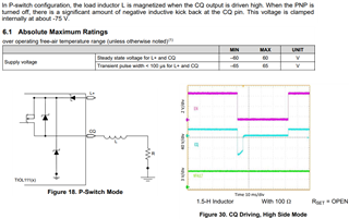
TIOS101 CQ pin abso max is ±65V(transient pulse width < 100us for VCC and OUT).
"9.2.2.3 Driving Inductive Loads" mentions a significant amount of inductive kick back is clamped internally at about ±75V.

How do we consider the relationship between ±65V and ±75V?

If we use inductive load and its significant amount of inductive kick back exceeds ±65V, TIOS101 has internal clamp diode so it is no problem even though it violates ±65V abso max?
±75V is not described in abso max spec so I'm not sure ±75V is just for protection.
±75V is just protection so we have to follow abso max spec or we can say that device can support up to ±75V under driving inductive loads?

Regards,
Kai

  • Kai,

    I've assigned this thread to one of our IO Link experts. But just as a quick observation, inductive kickback is a much shorter pulse time at +/-75V, where the 65V absolute maximum rating can be an indefinite bias.

    Please allow about 24 hours for the expert to comment as well.

    Regards,

    Eric Hackett 

  • Hi Kai,

    The TIOS101 is designed to handle inductive loads of up to 1.5H and detect, clamp, and drain the current in the inductive kickback. 

    As Eric has noted the 65V abs max is more of a DC specification and not necessarily the pulse transient voltage levels which can have high voltages for short periods of time.  The device can detect and clamp high voltage pulse transients to a save level, such as during an inductive kickback event, and then drain that current through these protection circuits.  These protection circuits will not detect a 75V DC voltage and therefore, this would cause damage to the device.

    The 65V abs max specification is slightly below the damage voltage of the device to provide a small amount of margin for process/voltage/temperature variance.  However, there is not much margin and the internal clamping voltage for the protection circuit is observed to be approximately 75V.

    Regards,

    Jonathan

  • Hi Jonathan,

    Sorry but I couldn't clearly understand your comment...

    Please let me simplify customer question then there are two customer questions.
    I attached customer wavefrom in attachment so could you take a look at it and support below questions?

    [Question 1]
    TIOS101 "voltage difference" is 60Vmax.
    from figure 9-12, VCC should be 24V and it seems VOUT_min is -80V so |VCC-VOUT|=104V, pulse width is ~4ms
    in customer case, VCC is 24V so |VCC-VOUT|=|24V-(-70V)|=94V, pulse width is ~10ms

    it seems both violates "voltage difference" abs max but can TIOS101 support customer waveform?
    If yes, could you let me know the reason?

    [Question 2]
    TIOS101 "supply voltage/ transient pulse width < 100us for VCC and OUT" is ±65Vmax.
    from figure 9-12, VOUT_min is -80V and pulse width <-65V seems ~4ms (>> 100us).
    in customer case, VOUT_min is -70V and pulse width <-65V seems ~6ms (>> 100us).

    it seems both violates "supply voltage/ transient pulse width < 100us for VCC and OUT" but can TIOS101 support customer waveform?
    If yes, could you let me know the reason?

    TIOS101_QA_0629.pptx
    Regards,
    Kai

  • Hi Kai,

    First off I want to be clear that the customer waveforms show the device is operating as expected.  There is no problem.  This is simply an issue of understanding how the device operates that I will try to be more clear in my explanation.

    The important distinction that needs to be understood is that there is a difference in the Abs Max voltage specification that is related to a DC voltage, and the voltage seen during a transient pulse such as an ESD, surge, or Inductive kickback or de-magnification event.

    We are talking about how the device handles a transient voltage pulse on the OUT pin that has a fast transition edge similar to an ESD pulse that can be as high as ±16kV, which is certainly higher than the DC abs max of ±65V. But we are not questioning how the device handles ESD pulses at this high voltage level because we generally understand that the device has cells that will clamp and drain this energy. 

    It needs to be understood that the device is handling the sudden negative voltage pulse from the de-magnetization of an inductor in a similar manner as it handles an ESD pulse.  The device detects the sudden change of the voltage using the edge of the pulse as a trigger, and then enables the internal protection clamping circuits to limit the voltage to a safe level and drain away the current.  Once there is no more current and the voltage is returned to normal and safe level, the clamping circuits are disabled.

    In the waveforms shown, the device clamps the voltage to approximately -75V as the safe voltage level and allows the current from the inductor to drain to GND.  This negative pulse width (time) will vary with the amount of current that needs to be drained and the current limiting resistor (100Ω), etc. and is the reason for the 4ms and 10ms observations.

    The supply voltage abs max specification that is being reference refers to voltages that do not transition fast enough to trigger the internal protection circuits.  I will admit that the description could be confusing when it states "Transient pulse width < 100μs for VCC and OUT" because it refers to the voltage as a "transient pulse."  However, this specification is referring to a pulse with a slower edge rate that is more common with a change in the DC supply voltage that would be too slow to trigger the protection circuits. 

    If the protection circuits are not triggered, the voltage seen by the internal circuits of the device will exceed the safe voltage levels and will cause damage to the device.  This specification is not intended to directly apply to the inductor de-magnetization event show in the customer waveforms.

    I hope this is a more clear explanation.

    Regards,

    Jonathan

  • Hi Jonathan,

    thank you for your clear explanation.
    we understood that customer waveform show the device is operating as expected.

    regarding internal protection clamping circuits, can we define the slew rate or transition edge rate that trigger internal protection circuit?

    Regards,
    Kai

  • Hi Kai,

    I think we can provide this information.  I don't currently have this information, but I will discuss this with the team and follow up with you.

    Regards,

    Jonathan

  • Hi Jonathan,

    Do  you get any comment from team?

    Regards,

    Kai

  • Hi Kai,

    I have not.  I apologize for the delay and I will contact them again and request a response.

    Regards,

    Jonathan