This thread has been locked.

If you have a related question, please click the "Ask a related question" button in the top right corner. The newly created question will be automatically linked to this question.

THVD8000: Help to review customer's schematic for THVD8000 application

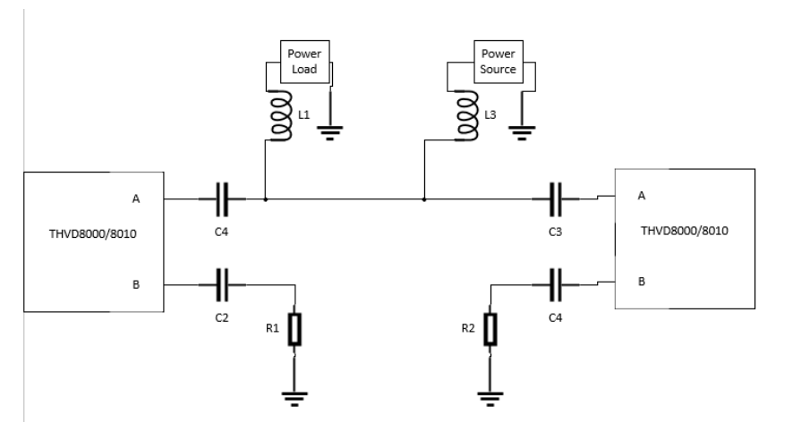
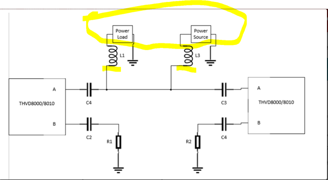
Part Number: THVD8000


Hi Team,

Our customer wants to use THVD8000 in one 24VAC Air Conditioner power line communication system, below is their schematic for THVD8000 section. Can you help to check if any issues and suggestions? Do we need the pull-up and pull-down resistor for A/B pins for our device?

  • Hi Jacky,

    Do you have a schematic with the power line + inductors as well as the inductance between the bus and power loads/power sources?

    Besides that I do have a few notes from what you have provided:

    1. First you do not need the pull-up / pull-down resistors on A/B unless you want to bias the bus to a specific DC level to help mitigate noise - its not a super common use case though so generally we don't see pull-ups/pull-downs included on A/B in most applications. It may not be a bad idea to have pads for resistors (and keep them DNI) in case a bias is desired as you or your customer go  through the design process.

    2. It seems you want to use this in a pseudo differential setup since B is connected to the common through a capacitor. A pseudo differential setup is possible but you do lose max distance as you are not going to get as large of a signal received (its about half of what you'd have in a true differential set-up). The issue with how it is setup now is that the "B" port cannot be connected to common/ground through a capacitor directly due to large possible transient currents so after the capacitor there needs to be a resistor to the common with a resistance equal to resistance from A to common* (power sources/power loads are considered "common" - but for this assumption to work there needs to be a capacitor between the AC source and common that will filter out the higher modulation frequencies  at the power source - this is always the case for DC as well but its less common for people to include a cap here for AC - and it needs to be there - it should be higher impedance at the AC source but lower impedance for the mod frequency - but with about 3 decades of frequency between standard power and the 125KHz mod frequency that you set it should be doable).

    3. The capacitors on A and B (C46 and C44) can probably be smaller - they okay since they meet the condition of being less than 5 Ohms at modulation frequency - but they could be a bit smaller to better block the lower frequency 24VAC voltage - so at 125KHz you can go as low as ~255nF and still meet the condition while providing more filtering for the 24VAC signal.

    4.  While the termination resistance is correct - I am not sure why there are so many resistors to meet this - this will add parasitics and board space that may not be necessary. This shouldn't hurt the application but I don't really understand why its there (I may  just be unfamiliar with this type of use case) - The split termination with capacitor is okay though.

    So I do have a few follow up questions:

    1. As mentioned before my review - I would really like to see the full bus and power connections if a schematic is available as the design of the THVD8000 requires system level knowledge - especially because I need to ensure that the inductors are sized correctly for the application. I only need to really see one node with power connections if the rest of the nodes are just copies. 

    2. What distance and how many nodes are present in the system ?

    Overall I think you have a good start - but there are a few things that could be fixed and a couple items that I would like to see to ensure the device is designed correctly with respect to the system.

    Also just as a note - we do have a really solid design guide: 

    https://www.ti.com/lit/an/slla496a/slla496a.pdf?ts=1656003083430&ref_url=https%253A%252F%252Fwww.google.com%252F

    This goes over how to size the inductors/capacitors and how the system level information all comes together. As mentioned above since the power source in this system is AC the only change is there needs to be a filter cap between AC main and common to filter out any data signal that may appear at the power load or source otherwise. But besides that it does have some solid information.

    And as a note I do have a diagram of the pseudo differential system (only 2 nodes are shown but more can be accepted on the bus):

    So if you could answer my above questions I'll be sure to check the rest of the schematic.

    Best,

    Parker Dodson

  • Hi Parker,

    Thanks for the detailed reply, please refer to attached customer's schematic which is intended to use for US market commercial A/C applications, and simplified application block diagram I drawn. Please help to review if we need to add the additional inductors on the 24VAC power line for indoor and outdoor boards. Any questions feel free to let me know.

    THVD8000_Power Bus_Hisense_6-23-2022.pdf

    Thanks.

  • Hi Jacky,

    I appreciate the schematic. 

    So I have a couple notes:

    1. There needs to be inductors between the power load and the bus and the power source. This would be L1 and L3 in the diagram above. Essentially the bus that combines the data and power needs to connected to power objects via inductors and the THVD8000's via capacitors. Everything power system needs to be behind the inductance. 

    From the schematic the power "load" would be everything  connected at X19 I believe - so there should be an inductor between the power/data bus and X19. Also where ever power connects to the bus - there needs to be an inductor as well.

    Since there are only two nodes in the system and you are using 1 wire you need 2 inductors. Since you have included termination the inductors (when combined in a parallel) need to have an impedance >= 375 Ohms. So an inductor with inductance of ~477uH at 125KHz will equal 375 Ohms - since there are two inductors needed you need to double that so each node should have an inductance value minimum of 955uH.  These equations are found in the THVD8000 datasheet + the design guide I attached in the last email for reference. 

    The only other concern I see is that after X19 there isn't a lot of capacitance - so the 125KHz modulation frequency signal could still show up at these nodes - using a capacitor from W to Common at X19 would help clean up the noise - it shouldn't be a problem for the THVD8000 - but it may cause system level noise that may not be acceptable for your application. 

    Once you have added the inductors in the system + add filter caps on Power Load (and power source if possible - so noise may exist there as well) + implement the notes I included in my first pass of the initial schematic I think it should be good to go.

    Please let me know if you have any other questions!

    Best,

    Parker Dodson