This thread has been locked.

If you have a related question, please click the "Ask a related question" button in the top right corner. The newly created question will be automatically linked to this question.

TCAN4550: Crystal Vp-p

Part Number: TCAN4550

I asked a few days about available registers without the crystal. Finally I received them, and assembled them.

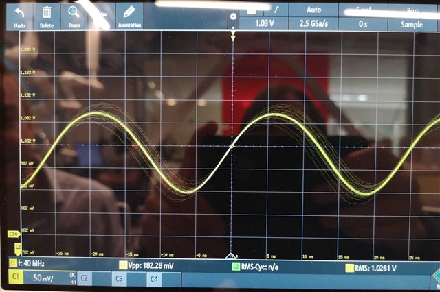
Part number: ABM11W40.0000MHZ8B1UT and 8pF caps.

However, I'm confused about the crystal spec in the datasheet. High level input between 0.85-1.1 VIO and Low <0.3 VIO.

VIO at 3.3 would be  L=<0.99V and H=>2.805V.

But on the scope (probing OSC1), i get 182mVp-p which swings around 1V.

Is this correct?

  • Hi Ole,

    Thanks for your question. We will get back to you on Monday with a response. 

    Regards,
    Eric Schott

  • Hi Ole,

    The TCAN4550 supports both a crystal oscillator or a single-ended clock input.  When a single-ended clock is used instead of a crystal oscillator, the signal is expected to swing between 0V and the VIO voltage (3.3V or 5V).  The High and Low Level Input voltage specs in the datasheet are for a single-ended clock input and are not applicable when a crystal oscillator is used. 

    When a crystal oscillator is used, the TCAN4550's Pierce Oscillator (transconductance amplifier) outputs a current to the crystal, but the voltage levels are set based on the components in the circuit and how the voltage dividers are created based on the resistive, reactive, properties of the components along with the phase delays in the circuit.

    There is an Automatic Gain Control / Peak Detector circuit that monitors the Vpp voltage of the OSC1 pin to help regulate the amount of current provided to the crystal that will generally try to maintain healthy Vpp and Vcm voltage levels on the signal. 

    The image you have shared looks like it is working correctly. 

    I will note that the TCAN4550 monitors the OSC2 pin for a "grounded" condition to indicate that a single-ended clock will be used instead of a crystal oscillator.  If the voltage on the OSC2 pin drops below the detection comparator threshold that is 100mV (typical) the device will disable the Pierce Amplifier and expect a single-ended clock to be provided on the OSC1 pin.  The comparator threshold will vary slightly between devices, but will be between 90mV and 150mV.  Therefore, you just need to ensure there is some margin on the OSC2 pin and that the minimum level of the waveform is greater than 150mV.  We recommend at least 100mV to 200mV margin to allow for variance from component tolerance in the circuit.

    More information can be found in this application note (Link).

    Regards,

    Jonathan