This thread has been locked.

If you have a related question, please click the "Ask a related question" button in the top right corner. The newly created question will be automatically linked to this question.

DS90UB948-Q1: Some circuit questions about 948

Part Number: DS90UB948-Q1

Hello Sir:

We are using 948 on our IVI project, we have some questions as below.

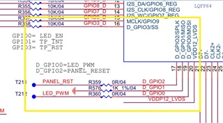
1. if pin 7, 8 and 9 were not use, does it need to pull low to GND by connecting 10Kohm?


2. If pin 17, 18 and 19 were not use, does it need to pull low to GND by connecting 10Kohm?

3. Can we reserve test points on LCD to outward pinning?

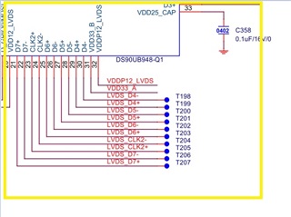
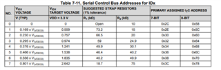
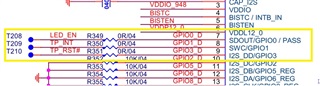
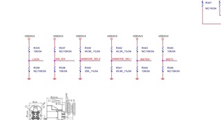
4. Can you help to check below configurations? anything wrongs? 

Please let us know your recommendations.

Thanks a lot.

  • Hi Statham,


    1. Pins 7, 8, and 9 need to be pulled down to ground. The 10K Ohm resistor will work.
    2. Pins 17, 18, and 19 also need to be pulled down to ground. The same resistance value will work.
    3. Pins 21-32 can be reserved for test points. The 100 Ohm termination for pairs (21-22), (23-24), (25-26), (27-28), and (29-30) will need to be done off the board. For pins 31 and 32, decoupling capacitors of 10 µF, 1 µF, 0.1 µF, and 0.01 µF need to connected from the pin to ground.
    4. The 948MODE_SEL0 and 948MODE_SEL1 voltage dividers are using the correct resistors. LOCK, BISTC, and BISTEN are currently setup for 1.65V which is lower than the 2V minimum for high level input. I would recommend choosing different resistors for the voltage divider to bring up the voltage. For the 948_IDX pin, please use table 7-11 in the datasheet to determine which I2C address you will be using. I will paste it below for your convenience.


    Regards,

    Jack Scherlag

  • Correction on item 4: The LOCK, BISTC, BISTEN, and 948_IDX pins are correct as is. I did not see the NC on the resistors at first. 

    Regards,

    Jack Scherlag