This thread has been locked.

If you have a related question, please click the "Ask a related question" button in the top right corner. The newly created question will be automatically linked to this question.

DS90UB941AS-Q1: LVDS display configuration

Part Number: DS90UB941AS-Q1

Hi,

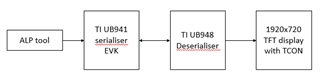
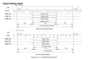
1. UB949 is able to get timing parameters right for the display (which require TCON to be configured) for the data coming from HDMI source.

2. Whereas with UB941 we are only able to generate test patterns successfully for that display but not the data coming from MIPI

We believe UB949 serializer is similar to UB941 apart from supporting HDMI instead of MIPI. In that case can we get configurations to get MIPI data to be
coming on the display without any TCON configurations (for now we arent having the support to configure TCON in our design hence wanted to utilize the test pattern generation method to get our mipi data in the display)

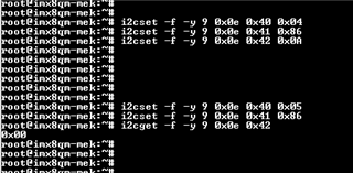
Below is the list of i2c registers we are writing to generate test pattern from UB941 serializer to the display
i2cset -y -f 9 0x0e 0x01 0x08 # REG:RESET_CTL --> Disable DSI
i2cset -y -f 9 0x0e 0x1E 0x01 # REG:TX_PORT_SEL --> Select FPD-Link III Port 0
# Auto-Scrolling Configuration
i2cset -y -f 9 0x0e 0x66 0x0F # Enable PGFT Register
i2cset -y -f 9 0x0e 0x67 0x1E # This sets the frame timer to 60
i2cset -y -f 9 0x0e 0x66 0x10 # Enable PGTSC Register
i2cset -y -f 9 0x0e 0x67 0x03 # This sets the number of active patterns to 3
i2cset -y -f 9 0x0e 0x66 0x11 # Enable PGTSO1 Register
i2cset -y -f 9 0x0e 0x67 0x43 # This sets Pattern 1 to Red (3) and Pattern 2 to Green (4)
i2cset -y -f 9 0x0e 0x66 0x12 # Enable PGTSO2 Register
i2cset -y -f 9 0x0e 0x67 0x05 # This sets Pattern 3 to Blue (5); Pattern 4 is ignored
# Set Pixel Clock(66.66 Mhz)
i2cset -y -f 9 0x0e 0x66 0x03 # enable PGCDC1 Register
i2cset -y -f 9 0x0e 0x67 0x03 # to set the clock divider to be 3 (200/87.96)
# set Active Frame Size (Horizontal width= 1920 pixels and Vertical width= 720 pixels)
i2cset -y -f 9 0x0e 0x66 0x07 # enable PGAFS1 Register
i2cset -y -f 9 0x0e 0x67 0x80 # to set desired Active Horizontal Width
i2cset -y -f 9 0x0e 0x66 0x08 # enable PGAFS2 Register
i2cset -y -f 9 0x0e 0x67 0x07 # to set desired Active Vertical and Horizontal Widths
i2cset -y -f 9 0x0e 0x66 0x09 # enable PGAFS3 Register
i2cset -y -f 9 0x0e 0x67 0x2D # to set desired Active Vertical Width
# Set Total Frame Size(Horizontal width= 2000 pixels and Vertical width= 758 pixels)
i2cset -y -f 9 0x0e 0x66 0x04 # enable PGTFS1 Register
i2cset -y -f 9 0x0e 0x67 0xD0 # to set desired Total Horizontal Width
i2cset -y -f 9 0x0e 0x66 0x05 # enable PGTFS2 Register
i2cset -y -f 9 0x0e 0x67 0xD7 # to set desired Total Vertical and Horizontal Widths
i2cset -y -f 9 0x0e 0x66 0x06 # enable PGTFS3 Register
i2cset -y -f 9 0x0e 0x67 0x2D # to set desired Total Vertical Width
# Set Back Porch. H Back Porch: 32 pixels, V Back Porch: 5 pixels
i2cset -y -f 9 0x0e 0x66 0x0C # enable PGHBP Register
i2cset -y -f 9 0x0e 0x67 0x20 # to set desired Horizontal Back Porch Width
i2cset -y -f 9 0x0e 0x66 0x0D # enable PGVBP Register
i2cset -y -f 9 0x0e 0x67 0x05 # to set desired Vertical Back Porch Width
# Set Sync Widths. H Sync Width: 16 pixels, V Sync Width: 2
i2cset -y -f 9 0x0e 0x66 0x0A # enable PGHSW Register
i2cset -y -f 9 0x0e 0x67 0x10 # to set desired Horizontal sync Width
i2cset -y -f 9 0x0e 0x66 0x0B # enable PGVSW Register
i2cset -y -f 9 0x0e 0x67 0x02 # to set desired Vertical sync Width
# Set Sync Polarities
i2cset -y -f 9 0x0e 0x66 0x0E # enable PBSC Register
i2cset -y -f 9 0x0e 0x67 0x03 # to set desired horizontal and vertical sync widths to "Negative"
# Internal Default Timing Configuration
i2cset -y -f 9 0x0e 0x65 0x05 # enable Auto-Scrolling with internal timing
i2cset -y -f 9 0x0e 0x64 0x11 # enable the pattern generator

i2cset -y -f 9 0x0e 0x01 0x00 # REG:RESET_CTL --> Enable DSI

Thanks & Regards

Musthafa av

  • Hello Musthafa,

    For debugging 941AS bringup, I recommend to follow this guide book: https://www.ti.com/lit/pdf/snla356 

    To be specific, please follow figure 3-2 which gives a step by step process to figure out where the problem is. Please let us know exactly where in the figure you are having an issue starting from the top and working down

    Here is a basic example script for 1920x720 for reference:

    # 1920x720p60, Dual Link FPD III
    # PCLK = 90.96MHz
    # DSI clock = 272.88MHz
    # DSI Lane Speed = 545.76Mbps/lane
    # 4 Lanes DSI
    # DSI input port 0
    # DSI non-burst mode with sync pulses 
    # MODE_SEL0 strap = No. 3
    # MODE_SEL1 strap = No. 0 or 1
    
    import time
    
    UB941AS = 0x18
    
    board.WriteI2C(UB941AS,0x01,0x02) # Reset
    time.sleep(0.1)
    board.WriteI2C(UB941AS,0x01,0x08) # Disable DSI
    
    board.WriteI2C(UB941AS,0x40,0x04) # TSKIP_CNT
    board.WriteI2C(UB941AS,0x41,0x05) # TSKIP_CNT
    board.WriteI2C(UB941AS,0x42,0x1A) # TSKIP_CNT
    
    board.WriteI2C(UB941AS,0x40,0x10) # Init DSI Clock Settings (From Section 10.2 of datasheet)
    board.WriteI2C(UB941AS,0x41,0x86) # Init DSI Clock Settings (From Section 10.2 of datasheet)
    board.WriteI2C(UB941AS,0x42,0x0A) # Init DSI Clock Settings (From Section 10.2 of datasheet)
    board.WriteI2C(UB941AS,0x41,0x94) # Init DSI Clock Settings (From Section 10.2 of datasheet)
    board.WriteI2C(UB941AS,0x42,0x0A) # Init DSI Clock Settings (From Section 10.2 of datasheet)
    
    board.WriteI2C(UB941AS,0x01,0x00) #Release DSI

    Best Regards,

    Casey 

  • Hi,

    +-------------+   4 lanes   +-------------+             +-------------+             +-------------+
    |        MIPI0|------------>|DSI0     OUT0|------------>|IN0     LVDS0|------------>|   TFT LCD   |
    |        I2C  |<----------->|I2C          |  FPD-Link3  |             | single OLDI |  1920*720   |
    |     SOC     |             |    UB941    |   2 lanes   |    UB948    |             |             |
    |             |             |             |     STP     |             |             |             |
    |   IMX8QM    |             |DSI1     OUT1|------------>|IN1          |             |             |
    +-------------+             +-------------+             +-------------+             +-------------+

    we are using ub941 serialiser and ub948 deserialiser, connections are made as shown above,
    we are using single MIPI DSI and dual FPD link and single OLDI output.
    could you please send the register configuration sequence that we need to do in serialiser as per the above mode and configuartion.
    and the registers that we need to modify in deserialiser for single oldi.

    Device tree:

    &i2c0_mipi0 {

                    #address-cells = <1>;

                    #size-cells = <0>;

                     pinctrl-names = "default";

                     pinctrl-0 = <&pinctrl_mipi0_lpi2c0>;

                    clock-frequency = <100000>;

                    status = "okay";


                    fpdlink_serializer_i2c0: serializer@0e {

                                    compatible = "ti,ds90ub941as_q1";

                                    reg = <0x0e>;

                                    reg_config = <0x01 0x08 0x1E 0x01 0x03 0x9A 0x1E 0x01 0x40 0x05 0x41 0x21 0x42 0x60 0x1E 0x01 0x5B 0x03 0x4F 0x8C 0x1E 0x01 0x40 0x04 0x41 0x05 0x42 0x0E 0x03 0x9A 0x01 0x08 0x17 0x9E 0x01 0x00>;

                                    status = "okay";

                    };


                    fpdlink_deserializer_i2c0: deserializer@2c {

                                    compatible = "ti,ds90ub948_q1";

                                    reg = <0x2c>;

                                    reg_config = <0x20 0x90 0x1F 0x09 0x1D 0x19 0x1E 0x90>;

                                    status = "okay";


                                    fpdlink_lvds_dic: fpdlink_bridge@100 {

                                                    compatible = "ti,fpdlink";

                                                    ti,dsi-lanes = <4>;

                                                    ti,lvds-format = <1>;

                                                    ti,lvds-bpp = <24>;

                                                    ti,width-mm = <508>;

                                                    ti,height-mm = <190>;

                                                    fpdlink-serializer-i2c-handle = <&fpdlink_serializer_i2c0>;

                                                    fpdlink-deserializer-i2c-handle = <&fpdlink_deserializer_i2c0>;

                                                    status = "okay";

                                                    display-timings {

                                                                    native-mode = <&timing0>;

                                                                    timing0: 1920X720_50HZ {

                                                                                    clock-frequency = <75193600>;

                                                                                    hactive = <1920>;

                                                                                    vactive = <720>;

                                                                                    hfront-porch = <40>;

                                                                                    vfront-porch = <31>;

                                                                                    hback-porch = <16>;

                                                                                    vback-porch = <5>;

                                                                                    hsync-len = <8>;

                                                                                    vsync-len = <2>;

                                                                    };

                                                    };

                                                    port@0 {

                                                                    reg = <0>;

                                                                    bridge_in: endpoint {

                                                                                    remote-endpoint = <&mipi0_host_out>;

                                                                    };

                                                    };

                                    };

                    };

    };

    Our TFT display is not using DE signal. it uses negative HS signal and negative VS signal.

    could you please let me know which are the registers needs to be set in serialiser and deserialiser along with vlaues.

    existing serialiser and deserialsier configurations are provided above in device tree.

    here i am attaching the input timing chart of TFT display

    could you please tell us the registers need to be configured in serilaiser and deserilaiser with respective values

    Thanks & Regards,

    Musthafa av

  • Hello Musthafa,

    I already provided an example script in my previous post. It is not clear to me from the above what operating mode your DSI source is in:

    - Non-burst mode with sync pulses

    - Non burst mode with sync events

    - Burst mode

    Can you clarify?

    Here is a new script with revised timing for the above you posted plus negative sync polarity:

    # 1920x720p50, Dual Link FPD III
    # PCLK = 75.19MHz
    # DSI clock = 225.57MHz
    # DSI Lane Speed = 451.14Mbps/lane
    # 4 Lanes DSI
    # DSI input port 0
    # DSI non-burst mode with sync pulses 
    # MODE_SEL0 strap = No. 3
    # MODE_SEL1 strap = No. 0 or 1
    
    import time
    
    UB941AS = 0x18
    
    board.WriteI2C(UB941AS,0x01,0x02) # Reset
    time.sleep(0.1)
    board.WriteI2C(UB941AS,0x01,0x08) # Disable DSI
    
    board.WriteI2C(UB941AS,0x40,0x04) # TSKIP_CNT
    board.WriteI2C(UB941AS,0x41,0x05) # TSKIP_CNT
    board.WriteI2C(UB941AS,0x42,0x14) # TSKIP_CNT
    board.WriteI2C(UB941AS,0x41,0x21) # DSI_CONFIG_1
    board.WriteI2C(UB941AS,0x42,0x60) # Set HS and VS polaritry active low
    
    board.WriteI2C(UB941AS,0x40,0x10) # Init DSI Clock Settings (From Section 10.2 of datasheet)
    board.WriteI2C(UB941AS,0x41,0x86) # Init DSI Clock Settings (From Section 10.2 of datasheet)
    board.WriteI2C(UB941AS,0x42,0x0A) # Init DSI Clock Settings (From Section 10.2 of datasheet)
    board.WriteI2C(UB941AS,0x41,0x94) # Init DSI Clock Settings (From Section 10.2 of datasheet)
    board.WriteI2C(UB941AS,0x42,0x0A) # Init DSI Clock Settings (From Section 10.2 of datasheet)
    
    board.WriteI2C(UB941AS,0x01,0x00) #Release DSI

    Best Regards,

    Casey 

  • Hi,

    we are using DSI0 port only ,

    like you suggested i have done the steps.

    but it is not reflecting value is always 0.

    i have given the serialiser register configurationn in our linux device tree as shown the previous discussion

    thanks & Regards,

    Musthafa av

  • Musthafa,

    Why are you setting reg 0x86 in the indirect reg page 0x40 = 0x04? The above code sets register 0x86 in the indirect page of 0x40 = 0x10

    Best Regards,

    Casey 

  • root@imx8qm-mek:~#
    root@imx8qm-mek:~#
    root@imx8qm-mek:~# i2cset -f -y 9 0x0e 0x40 0x10
    root@imx8qm-mek:~# i2cset -f -y 9 0x0e 0x41 0x86
    root@imx8qm-mek:~# i2cset -f -y 9 0x0e 0x42 0x0A
    root@imx8qm-mek:~#
    root@imx8qm-mek:~#
    root@imx8qm-mek:~#
    root@imx8qm-mek:~# i2cget -f -y 9 0x0e 0x42
    0x00
    root@imx8qm-mek:~#
    root@imx8qm-mek:~#

    there is no change in display by the above changes and its not reflecting also

    we are using DSI0 port only. DSI_CONFIG_1 and TSKIP registers are configured from device tree itself.

    kindly refer the device tree reg_config , please revert us back if we made any mistakes.

    thanks & Regards,

    Musthafa av

  • Musthafa,

    Have you even confirmed that basic I2C communication to the 941AS device is working? For example if you read back register 0x00, do you receive 0x1C?

    Best Regards,

    Casey 

  • yeah basic i2c read write is working
    i can able to generate pattern also by using pattern generation control registers

  • Musthafa,

    It doesn't look like your device tree config matches what I gave before. This is what you have:

    0x01 0x08 0x1E 0x01 0x03 0x9A 0x1E 0x01 0x40 0x05 0x41 0x21 0x42 0x60 0x1E 0x01 0x5B 0x03 0x4F 0x8C 0x1E 0x01 0x40 0x04 0x41 0x05 0x42 0x0E 0x03 0x9A 0x01 0x08 0x17 0x9E 0x01 0x00

    The way I interpret this is register, write value, register, write value, repeated. If so, the instead it should be:

    0x01 0x08 0x40 0x040x41 0x05 0x42 0x14 0x41 0x21 0x42 0x60 0x40 0x10 0x41 0x86 0x42 0x0A 0x41 0x94 0x42 0x0A 0x01 0x00

    I also see what you are saying about the 0x86 and 0x94 indirect regs not reading back the written value but I have to dig deeper on this. I seem to recall they are write only but not read. Anyways I don't think that has anything to do with your issue here. 

    When you got PATGEN working, which was that?

    - PATGEN with internal timing and internal clock?

    - PATGEN with internal timing and external clock?

    - PATGEN with external timing and external clock?

    I am trying to see where you are on this debug flow chart:

    Based on where you get stuck we can determine where exactly to look. 

    Best Regards,

    Casey 

  • Hi,

    we are using UB941 and UB948 with Dual link FPD and single OLDI configuaration.
    LVDS channel is connected with our TFT dsiplay of resolution 1920x720

    and that is working on HV mode

    there is no DE signal.

    so how can we enable HV mode and disable DE mode in 941 serilaiser and 948 deserialser.

    Thanks & Regards,

    Musthafa av

  • Musthafa,

    There is no such thing as DE mode vs. HS/VS mode in the 941AS. The 941AS always generates DE, HS, and VS signals and then if the panel uses DE only, then the HS/VS signals are simply ignored. 

    Can you please respond to my previous question about your progress on the bringup flow chart? To help you debug this issue I need to know specifically which step in the flow chart you are getting stuck on starting from the top and working down the list 

    Best Regards,

    Casey