This thread has been locked.

If you have a related question, please click the "Ask a related question" button in the top right corner. The newly created question will be automatically linked to this question.

DS90UB948-Q1: SPI configuration

Part Number: DS90UB948-Q1

hi,

+-------------+   4 lanes   +-------------+             +-------------+             +-------------+
|        MIPI0|------------>|DSI0     OUT0|------------>|IN0     LVDS0|------------>|   TFT LCD   |
|         SPI |<----------->|SPI          |  FPD-Link3  |             | single OLDI |  1920*720   |
|     SOC     |             |    UB941    |   2 lanes   |    UB948    |             |             |
|             |             |             |     STP     |             |             |             |
|   IMX8QM    |             |DSI1     OUT1|------------>|IN1      SPI |------------>| SPI         | 
+-------------+ +-------------+ +-------------+ +-------------+


How to enable SPI pins and SPI communication between serialiser and deserialiser
we are using ub941 seriliaser and ub948 deserialiser
which are the registers needs to be configured on ub941 and as well as ub948?
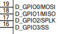
we need to implement spi commuincation from Application processor to TFT display as shown in the above image.
kindly revert back asap on this

Thanks,
Musthafa av
  • Hello Musthafa,

    Sections 8.3.9 to 8.3.10 in the 941 datasheet and Sections 7.3.9 to 7.3.10 in the 948 datasheet summarize SPI implementation on those devices. Nevertheless, we will get back to you tomorrow with specific registers and values.

    Best regards,

    Abdulrahman Tabbaa

  • Hello Musthafa,

    Before enabling SPI there must be a valid LOCK between 941 and 948. Also, the 941 and 948 must be configured in FPD Dual mode. After that, to configure SPI, perform the following:

    1) Set the PORT1_SEL bit in register 0x1E in the 941

    2) Configure register 0x43 on the 948 with the SPI polarity you wish, but make sure bits [2:0] are 0b110

    3) D_GPIOs 0, 2, and 3 are inputs in the 941 and D_GPIO1 is an output. Therefore, in the 941, write 0x03 to register 0xD, 0x31 to register 0xE, and 0x03 to register 0xF.

    4) D_GPIOs 0, 2, and 3 are outputs in the 948 and D_GPIO1 is an input. Therefore, in the 948, write 0x01 to register 0x1D, 0x13 to register 0x1E, and 0x01 to register 0x1F.

    There are additional timing SPI configurations in registers 0x60 to 0x62 in the 941. Hope this helps.

    Best regards,

    Abdulrahman Tabbaa