This thread has been locked.

If you have a related question, please click the "Ask a related question" button in the top right corner. The newly created question will be automatically linked to this question.

SN65HVD09: SN65HVD09 - EMC problems

Part Number: SN65HVD09

Hello, 

we had the emc test with our new product last week. On this product also sits a SN65HVD09.
All 9 channels are occupied and the function is basically given. We control a RGB LED matrix display and need besides the RGB channels also 2 clock signals, a latch signal and control signals.

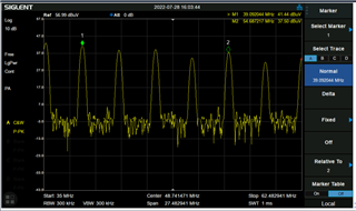
The clock signals have a frequency of 4MHz (see oscilloscope picture).From my point of view, the signals on the RS485 side look quite good and even with a longer line the edges are still steep enough to be detected safely.

On the original image from the test lab, the limit has been exceeded in some places in the range from 30MHz to 100MHz.
As it turned out, these peaks come from the SN65HVD09

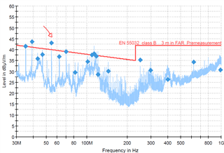
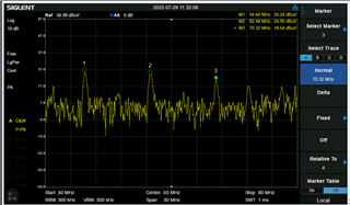
Back in the office, we used a near-field probe and a spectrum analyzer to remeasure the situation. Even with an EMI Antenna from 3m away, the interference levels can be seen. However, we can't find the reason why the SN65HVD09 is radiating so much at this point. When we switch it off, all interference levels are gone. 

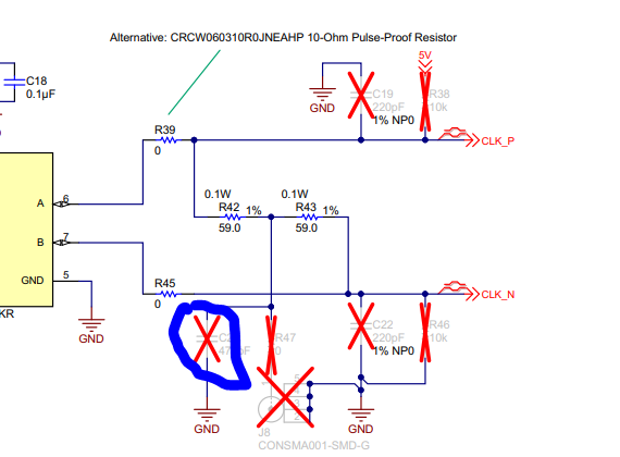
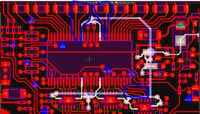
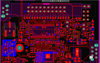
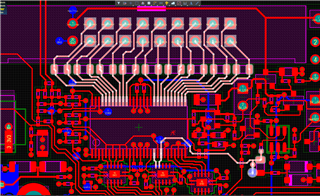
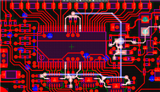
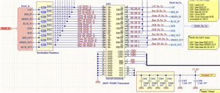
Here is the layout and the schematic:
the marked lines (top layer) are the 5V supply lines. Layer 2 has GND throughout and layer 3 has 3.3V throughout.

We are grateful for any input and do not know where we could optimize.
Thanks already for the help

Boris

  • The SN65HVD09 generates edges that are fast enough for 20 Mbps.

    You could slow down the edges with ferrite beads, and/or remove common-mode noise with common-mode chokes.

    On the schematic, the A/B signal routing does not look very symmetric, and the board detail does not show it at all. Please show all nets/traces for the A/B signals in the schematic and the board.

  • Hi Boris,

    So first from a schematic perspective replacing the 120 ohm resistors with 2 60 Ohm resistors and a capacitor to create a split termination. That is our general advice for EMC considerations that don't typically have much negative effect on the system. The use of Ferrite beads on the line also are a popular solution. 

    Image with DNI'd EMC elements shown - I circled the split termination (470pF cap)  (the other options shown aren't great for higher speed applications) 

    From a layout perspective I have circled a few things (this may be hard do the the high density nature of the application  - but I still want to point it out)

    The clock lines (two 2 blue circles) aren't the same length and that discontinuity could be causing SI issues that could lead to EMC issues. Ideally all RS-485 differential traces are the same length and differentially coupled which also doesn't seem to be the case (as the distance between lines varies - this should be minimized as much as practically possible) 

    The bottom left blue circuit just has some weird bends in it - it seems to be due a mechanical outline - if possible remove those bumps.

    In general the idea is to mitigate reflections and/or filter out high frequency signals (without overloading the driver) - the more reflections the more likely  there will be EMC issues. 

    To mitigate reflections / clean up higher frequency signals:

    1. Keep spacing between differential line pairs as consistent as possible.

    2. Ensure board thickness between microstrip lines and ground plane produce a characteristic impedance of ~120 Ohms

    3. Use termination (which is already done) and if extra filtering is needed make the termination a split termination 

    4. Avoid sharp turns (smooth turns and as few turns as possible - the straighter the microstrip routing the better as curves can change the impedance and sharp corners will radiate pretty efficiently) 

    5. Additional ferrite beads on both the A and B lines can also be used to help attenuate higher frequency signals.

    These steps will help remove higher frequency energy and will help prevent reflections (and reduce the ones that remain)

    Please let me know if you have any other questions!

    Best,

    Parker Dodson. 

  • Hey Clemens, 

    thanks for your answers! The common mode chokes are a good idea. 

    All A/B signals are going to the connector and then after about 50cm length to the led panel. 

    in the second picture you see the A/B signals in detail. And at the bottom from the driver the clock input pins. One of the clock signal is also the input from an hardware watchdog -  i know, the trace/ the stub is not the best but we need the watchdog. 

    i will give you a feedback if the emc results are getting better

    Greetigs from Germany

    Boris 

  • Hey Parker,

    thank you very much for the quick and detailed answer.
    You are absolutely right with your hints about the layout.

    • At this point I have forgotten the impedance routes.
    • The common mode chokes were initially planned and have been omitted due to lack of space.
    • The split termination resistors are also a good idea, although I haven't had the best experience here in the past.
    • I will try to implement your advice on the existing board and keep you up to date with new measurement results.

    Thanks and greetings from Germany
    Boris

  • I guess the cable to the LED panel does not use twisted pairs? Try shielding it (wrap it in aluminium foil).

    If the transmitters are always active, then you do not need the termination resistors on this board.

  • Thanks Boris!

    I will leave the thread open - I am hopeful some of these changes suggested by me and Clemens are helpful! I will be here if you have any further questions for when you have some more data.

    Best,

    Parker Dodson