This thread has been locked.

If you have a related question, please click the "Ask a related question" button in the top right corner. The newly created question will be automatically linked to this question.

DP83867E: Erratic Behavior/Hardware Problem

Part Number: DP83867E


Hello,

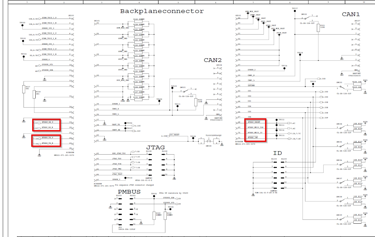
we use DP83867ERGZT on a backplane board connected to Arria 10 FPGA via SGMII.
FPGA is located on detachable add-on PCB. We use two supply configuration (VDDA1P8 pin are NC), VDDIO is 1.8V.


The PHY worked well for a long time, but now we have issues on 3 backplanes.
If a backplane with a "healthy" PHY is turned on w/o FPGA, than the PHY boots up and can establish MDI connection to the link partner.
If a backplane with a probably damaged PHY is turned on w/o FPGA, than the PHY seems to be deactivated:

  • Vrbias = 0V
  • VDDA1P8 = 0V
  • RESET# is low (no external PU)
  • INT#/PWDN# = 320mV (2.2K external PU to VDDIO)
  • 25MHz clock is running (1.8V oscillator)

What can pull RESET# and PWDN# low and prevent PHY from booting up if no MAC is connected?

Thanks in advance.

  • Hi,

    What was changed when the design stopped working? It is extremely rare that an untouched design would operate for a long time and start failing on 3 separate boards.  

    I would have to see a schematic to know what can pull these pins low. Can you provide this?

    Thanks,

    David

  • Hi David,

    there were no design changes. The boards were manufactured in 2019. As far as I know, one board had this issue almost from the beginning. For two other boards, the issue came up couple of months ago.

    I attached two relevant schematic pages: backplane connector and PHY. These PHY signals are connected to the backplane connector:

    ETHBP_MDIO_IO

    ETHBP_MDIO_CLK

    ETHBP_INT

    ETHBP_RESET

    ETHBP_RX_P/N

    ETHBP_TX_P/N

    Only ETHBP_MDIO_IO and ETHBP_INT have external PUs to VDDIO, all other signals are floating if no FPGA is attached to the backplane connector.

    /cfs-file/__key/communityserver-discussions-components-files/138/DP83867E_5F00_1.jpg

    /resized-image/__size/0x240/__key/communityserver-discussions-components-files/138/DP83867E_5F00_2.jpg

    Regards,

    Viacheslav

  • Hi Viacheslav,

    The 2nd image is extremely pixelated, can you send a higher quality version?

    Are all 3 boards identical? Did anything change a few months ago when the issue started appearing?

    Thanks,

    David

  • Hi David,

    here is PDF schematic.

    DP83867E.pdf

    Yes, all 3 board are identical. The only change was that sometimes the boards were transported to another biulding (of course using ESD protective bag or box). I can't imagine it is an ESD damage.

    Regards,

    Viacheslav

  • Hi Viacheslav, 

    I will review the schematic and get back to you within 5 business days.

    Thanks,

    David

  • Hi Viacheslav,

    The schematic shows you are using a center tap connected magnetic, which is against the datasheet requirement in section 9.2.1.1, which could be a cause of some sporadic issues.

    Can you please describe the failure condition in more detail? Is the PHY completely off? Can you read/write registers, or see a signal on RX_CLK pin? Are you probing the reset pin and finding it to be low? If so, please install a pullup resistor of 2.2kohm and see if the issue is resolved.

    Thanks,

    David

  • Hi David,

    thanks for the advice regarding center pad connection. I can try to replace the RJ45 connector, but the new connector will not be pin-compatible because of additional pins for center tap connections.

    I'm comparing two backplanes - first with a healthy PHY, second with a damaged PHY. I don't connect the FPGA to the backplane, so read/write registers is not possible. We don't have a possibility to connect an external MDIO adapter.

    A backplane with a healthy PHY - PHY boots up and establishes MDI connection to the link partner.

    A backplane with a damaged PHY - PHY seems to be off competely because 

    • Vrbias = 0V
    • VDDA1P8 = 0V
    • RESET# is low (no external PU installed)
    • INT#/PWDN# = 320mV (2.2K external PU to VDDIO)

    I installed external 2.2K pull-up to VDDIO on RESET# pin - no changes, measured voltage is 250mV.

    I also connected the external VDDIO=1.8V to the VDDA1P8 pins (three-supply configuration) - no changes too.

    Regards,

    Viacheslav

  • Hi Viacheslav,

    It sounds like there are other issues with your backplane, causing the PHY to not be powered and reset. 

    The Reset and INT/PWDN pins needs to be held high for the device to operate. If an external pull resistors is not pulling the voltage above the Vih level, this is a problem with your backplane, not the PHY, and should be resolved there.

    Thanks,

    David

  • Hi David,

    I don't agree with your statement. I don't see any problems on the backplane that can prevent PHY from powering up.

    All external voltages (2.5V, 1.1V and VDDIO=1.8V) are stable with clean start-up edges.

    I don't see any spikes on the voltage rails. The voltage regulator is capable to provide 1A on each rail. 2.5V and 1.1V are used exclusively for DP83867, no other consumers are connected. 1.8V are connected to DP83867, to a couple of level shifters, and to a FTDI IC used for serial communication. All of these components don't have high current consumption to overload the 1.8V rail.

    In principle, the PHY needs only 3 voltages and the reference clock to power up. An external pull-up is only requiered on the MDIO pin. All other pins have internal pull-ups or pull-downs according to the datasheet. A proper working PHY pulls up the RESET# signal internally w/o installed external resistor (RESET# green, INT#/PWDN# red).


    That's why I'm thinking that RESET# and INT#/PWDN# are pulled down internally. There is an internal POR circuit (datasheet 8.5.5). How does it work? Can this circiut be damaged? What are the criteria for straring the normal operation after power up?

    Regards,
    Viacheslav

  • Hi Viacheslav,

    Please send the results of the impedance measurement of RESET and INT pins on 1 good backplane and 1 bad backplane. 

    Also send the results of the bad backplane reworked with a known good PHY. 

    Thanks,

    David

  • Hi David,

    here are the results of the impedance measurement. No power was applied and no external components were connected to RESET# and INT#/PWDN# pins during measurement.

    On the good backplane the both pins are high impedance 700-800 kohms. If the pin is damaged, the impedance decreases to 300-400 omhs. Pulling the damaged pins above Vih with 100 ohms resistor makes the PHY fully functional again (tested on SN04). Only the INT# pins seems to be damaged on SN03.

    SN01 (good) SN03 (bad) SN04 (bad) SN05 (bad)
    RESET# 760 kohms 700 kohms 350 ohms 420 ohms
    INT#/PWDN# 800 kohms 490 ohms 440 ohms 360 ohms

    Could this be an ESD damage? All pins are protected with 2.5KV according to the datasheet (section 7.2 ESD Ratings). But why are only these pins affected? Could the internal protection on these pins be weaker?

    Regards,

    Viacheslav

  • Hi Viacheslav,

    This does sound like a damaged pin/device. It is difficult for me to say where the damage came from, though. You are correct, all pins are protected from 2.5kV of ESD. It is possible there was an ESD event that exceeded this specification. Was there any other event that you can correlate the start of improper operation with?

    Please perform a rework of a bad part with a known good part and let me know the results. 

    Thanks,

    David