This thread has been locked.

If you have a related question, please click the "Ask a related question" button in the top right corner. The newly created question will be automatically linked to this question.

TCAN4550: crystal and capacitor problem

Part Number: TCAN4550

Hi Team,

we have some issues in relation with TCAN and crystals and your help would be highly appreciated. We would need your expert team in this case, because it is urgent.

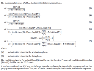
We have problems with not working CAN communication on 1% of the tasted PCBAs. So far, we have assembled more than 20K units. Lately we are also experiencing reclamations the units which went through all the tests OK are coming back not working.  We assume that crystal calibration/matching on the PCB is not made properly and therefore we are experiencing these problems.

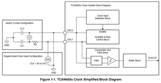
The Crystal HKC2016SX-40MHZ-31303-R4V1 is used for the clock on the TI TCAN4550RGYRQ1 with load capacitors 6pF.

The signal carrier frequency on the CAN bus is not shifted. The problem is that on unstable PCBAs/crystals communication sometimes it is working and then it stops, or it never starts.   

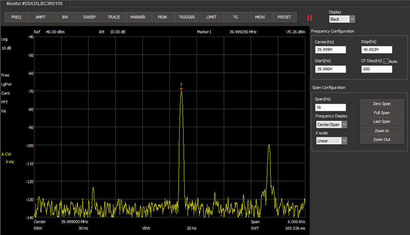
From the measurements of the crystal frequency with spectrum analyzer we don’t see a shift in crystal frequency:

What we have detected is that if we heat or cool down the unstable PCBA the CAN communication starts to operate normally.  Or if we touch the load capacitors with the finger the CAN communication starts for a while.


Any help will be appreciated.

Thank you!

Seba

  • Hi Seba,

    We assume that crystal calibration/matching on the PCB is not made properly and therefore we are experiencing these problems.

    I completely agree with this statement and I understand the situation you are facing.  However, while you have focused on the frequency side of the crystal and loading caps, this is not the reason for the communication stability issues you are facing.  I have written an application note that discusses this in greater detail.  Here is the (link).

    The issue is that the drive level, or the power dissipated across the crystal, is likely too high.  This results in a large mechanical vibration and produces a large oscillating voltage.  The TCAN4550 has a peak detector and an automatic gain control circuit to help control the amount of current it sources through the crystal so that it will maintain an ideal oscillation waveform voltage, but it does have its limitations and works best across certain external loads (capacitors value and ESR, resistance or ESR crystal values, etc.) and there is a minimum current level it must source when enabled.

    In your case this external load of the crystal, caps, PCB trace resistance and capacitance, etc. is such that the TCAN4550 can't reduce the output current to lower level and reduce the drive level.

    The communication issues come from the TCAN4550's single-ended clock detection comparator which is monitoring the OSC2 pin for a "grounded" pin or a voltage less than approximately 100mV.  The actual threshold could vary between 90mV and 150mV, but it is typically around 100mV.  If the voltage on the OSC2 pin crosses this threshold, then the comparator will disable the crystal oscillator amplifier and switch the device to single-ended detection mode where it expects a clock to be applied to the OSC1 pin.

    During this time, the device will not have a valid working clock to to drive the digital core and communication will fail.  The crystal will continue to oscillate, but the waveforms will decay because of the parasitic losses in the circuit, and the amplifier is not injecting new current to compensate for the losses.  Once the waveform levels are small enough that the OSC2 voltage is above the comparator's detection threshold, the device switch back to the crystal oscillator mode,current is applied to the crystal again, and communication is again possible because the digital core has a clock signal.

    A large oscillation waveform voltage on the OSC2 pin resulting from a high crystal Drive Level can cause the lowest peak voltage of this waveform to cross this detection threshold.  Therefore we need to reduce the OSC2 peak-to-peak amplitude to keep the voltage above this detection threshold window and create some margin as well for safety.

    So how to prevent this, or what can we do about it?  To reduce the voltage waveform we need to reduce the mechanical vibration in the crystal, which means reducing the drive level.

    The Drive Level  is defined as:

    Therefore, we need to reduce either the source current, or the total Resistive load. 

    The recommended method to reduce the current flowing through the crystal and load capacitors is to add a series dampening resistor between the OSC1 (amplifier output) and the crystal to restrict the current flow.  If a resistor is not already included in your schematic and board layout, this is not an option.  Typical values for this resistor are in the 100-300 ohm range, but vary with the application.

    If there is not a series dampening resistor between OSC1 and the crystal, and since the automatic gain control and peak detector circuit will ensure the device is already outsourcing the minimum amount of current possible, we can't reduce the current level so we will need to reduce the Rload.

    Rload is defined as:

    Rm is the motional resistance of the crystal, and C0 is the shunt capacitance of the crystal, we can't adjust those parameters.  Therefore, we need to adjust Cload or the load capacitance. Because Cload is in the denominator of this equation, increasing Cload will decrease the value of Rload, and therefore reduce the Drive Level.

    Cload is the total capacitance from the load capacitors, the OSC1 and OSC2 pin capacitance, and the PCB parasitic capacitance.  The pin and parasitic capacitance is not temperature stable and can change with temperature, but it is also not something we can easily change or control either.  Therefore we can only control the values of the load capacitors.

    Increasing the capacitor values from 6pF to either 8pF or 10pF should reduce the Rload enough to create the margin needed to eliminate the clock stoppage and communication issues.  You may need to try a couple of values to determine what values you need.  You can monitor the OSC2 waveform with a high impedance, and low capacitance probe to verify the voltage change.  The probe capacitance will add to the board capacitance, so the minimum peak voltage level will appear higher than it will be when the probe is not connected, so take note.

    Your observations of changing temperature or touching the load capacitors is proof that changing the load capacitance will improve the circuit.  The temp will change the PCB parasitic capacitance because it is not temperature stable, and your finger will add a lot of capacitance.  The added capacitance of a scope probe on OSC2 is also likely enough to cause a failing board to start working correctly.

    However, while changing the capacitors will help the stability, it will cause a small frequency shift, so we don't want to shift it more than is necessary to ensure stability.  The CAN standard should allow for a large enough frequency tolerance that we should not violate this spec with this capacitor increase.

    If however, a total load capacitance increase can't be tolerated with a symmetrical increase to both load cap values, it may be possible to adjust the cap values to an asymmetrical loading (increasing one and decreasing the other) that will adjust the voltage levels of the signal at each side of the crystal by changing the voltage dividers set by the crystal and capacitor resistance and reactance, properties.  This is not the recommended method due to the impact on the overall oscillation waveform, but it can allow some tuning without adding additional capacitance and frequency shift.

    I know this is a lot of information, but hopefully it gives you all the information you need to understand and resolve your issue.  It is recommended to have about 200mV of margin between the maximum comparator detection threshold of 150mV and the lowest peak voltage of the OSC2 waveform.  So if you can adjust the circuit such that the OSC2 min level is about 350mV, should not see any stability issues.

    Regards,

    Jonathan

  • Hi Jonathan,

    Thank you very much for quick and detailed response. Now the whole thing is a little bit more clear.

    Increasing resistor is not an option because we do not have it.

    Increasing the capacitor values from 6pF to either 8pF or 10pF should reduce the Rload enough to create the margin needed to eliminate the clock stoppage and communication issues. 

    Yours statement correctly correspond, with what we already tried. We raised capacitance and PCB was immediately more stable and more durable in high temperatures. We did not want to take this action because there was quite of frequency shift (as you already stated) sometimes also 1000Hz.

    The only question for now is how much frequency deviation can TCAN4550 handle, can you help me find this data please? I understand that higher bus frequency should be more affected by higher frequency deviations on crystal. 

    Our system is using:

    - communication speed is 500kb/s

    - nominal bit rate prescaler is 2

    - nominal time quanta before sampling point is 24

    - nominal time quanta after sampling point is 16

    Regards.

    Seba

  • Hi Seba,

    The amount of frequency deviation is somewhat system dependent and it is specified in the ISO 11898-1 specification in section 11.3.2.5 as:

    The Tolerance of a node clock oscillator frequency fosc around the nominal frequency fnom shall be given by the range [(1-df) x fnom ≤ fosc ≤ (1 + df) x fnom]. The tolerance df depends on the length of the time quantum, the segments of the bit time, and on the synchronization jump width.  The maximum difference between the ode clock oscillators of any two nodes shall be 2 x df x fnom.

    The maximum tolerance df of fosc shall meet the following conditions:

    I understand that you are only using Classical Frames based on your 500kb/s data rate.  If so, you should only need to be concerned with the first two equations (3 and 4). I also don't know what your synchronization jump width setting is, but typically it is the same as your Phase_Seg2 (time quanta after the sample point). 

    Doing some basic calculations using these numbers with a CAN Bit Timing spreadsheet tool, I'm getting a 1.59% for the allowed oscillator tolerance on a 40MHz frequency, which is a maximum deviation of 636,000 Hz.

    The minimum crystal oscillation frequency would be 39.364MHz, and the maximum would be 40.636MHz.

    Obviously we don't want to operate at the extremes, but at a low data rate such as 500kbps, there should be enough margin to tolerate the small frequency shift of 1000Hz from the higher load caps. 

    The allowed tolerance decreases with faster data rates and just as an example, I'm also calculating a CAN FD 5Mbps data rate that only has 8 time quanta per bit period and the tool is returning an allowed tolerance of 0.31% which is deviation of 124,000 Hz on a 40MHz frequency.  Therefore, a few kHz of deviation would still be acceptable at these data rates.

    Regards,

    Jonathan

  • Hi Jonathan,

    Raising the caps solved the problem. 

    With this calculations we are safely within the operating ranges, we are not observing any issues in communication.

    I must say that we had troubles to measure this crystal. Can you maybe suggest which probe is good for measuring?

    We try with:

    https://www.batronix.com/shop/measurement/probes/Micsig-DP10013.html

    Regards.

    Seba

  • Hi Seba,

    I am glad to hear that the problem is resolved. 

    Making measurements on a crystal oscillator circuit is definitely difficult, regardless of the probe, because the resistance and capacitance of the probe alters the delicate balance of the oscillator and the voltage dividers created by the resistive and reactive properties of the components.  I don't have a specific recommended probe, but an active FET based probe with a high input impedance and lowest capacitance should be used to minimize the loading and improve the accuracy.  The probe you referenced looks to have decent specifications with 2.5pF or less of capacitance and greater than 4Mohms of impedance.  I've seen some high-end probes from Tektronix and other vendors that have less than 1pF of capacitance, but I don't have a part number to share.

    There are some tricks you can play to somewhat calculate out the impact of the capacitance of the probe.  You can make a measurement with the probe, and then add an additional capacitor to the circuit that is equal to the probe's capacitance and make another measurement.  Assuming the signal shift is somewhat linear with the capacitance increase, you can take the difference between the two measurements to know how much the signal shifts by the additional 2.5pF.  This difference should represent the equivalent impact to the signal when a probe is applied by itself and allow you to subtract this difference from your original measured number.  This result should give you an idea of what the signal looks like when there is not a probe attached.

    Making some incremental measurements with different capacitors can help determine the linearity of the shift based on this approach if you want to be more accurate, but this is the general idea of how to calibrate out the effects of the probe.

    Regards,

    Jonathan