This thread has been locked.

If you have a related question, please click the "Ask a related question" button in the top right corner. The newly created question will be automatically linked to this question.

DS90UB954-Q1: How to improve the insertion loss of FPD-Link

Part Number: DS90UB954-Q1

Hello,

     I am using DS90UB954-Q1 as a deserializer, in Power Over Coaxia confuguration. The filter circuit is shown in picture1.

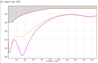
     This filter circuit simulation meets the requirement of FPD-Link insertion loss, as picture1 shows.

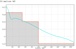
     However, in 2.5D PCB simulation,it fails the criteria, see picture 2. 

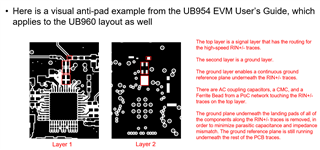
     My layout of Power Over Coaxia as picture 3 shows:

     What should I do to improve the Insertion Loss?

Looking forward to guidance !

  • Hello Zhang,

    Typically, a major factor in Insertion Loss is impedance mismatch along the high-speed trace. Our FPD-Link devices require a tightly-controlled single-ended impedance of 50-Ohms (+/-10%) for the RIN+ and RIN- traces of the 954. In order to achieve this impedance, there must be a continuous ground plane underneath the entire high-speed PCB trace. There must also be ground cut-outs underneath the landing pads of any components along the high-speed path, such as AC coupling capacitors, ESD diode, and the PoC component that is touching the RIN+ trace. This is because the landing pad's increased width will increase the impedance of the PCB trace and may cause impedance mismatch outside of the allowed 50-Ohms (+/-10%) range. There will also be increased parasitic capacitance between the landing pads, which will affect the data being transferred on the high-speed path.

    There are also several layout guidelines that we recommend as well, such as routing the RIN- trace along the RIN+ trace, all the way up to the connector if you are routing on a Top/Bottom layer, in order to introduce a differential nature and minimize EMI/EMC. Please see Section 10.1 PCB Layout Guidelines in the 954 datasheet for the full details.

    The image that you shared is too small for me to review in detail. If you would like, you may provide your layout files and request a Layout Review. But keep in mind this is a public forum, so you may need to message me separately.

    One thing I also noticed is that I don't recognize the PoC network that you are using in the first picture you shared. If customer is using a custom PoC network in their design, then they will be responsible for verifying that it will not have a significant impact on their system. We have a recommended PoC network in the 954 datasheet, which was verified to work in a 4G and 2G Forward Channel line rate and supports up to 150mA of current draw through the PoC network.

    Best,

    Justin Phan

  • Appreciate for your answer!

    Our PoC network needs to work at a current of 300mA, so the recommended PoC network in the 954 datasheet is inappropriate.

    Our simulaton of return loss met the requirement, and insertion loss also passed in the high frequency, namely 1Ghz to 2.1Ghz. I think these results can prove that there is no serious mismatch in impedance. But it is strange that insertion loss failed in low frequency(25Mhz to 1Ghz).

    I now suspect that the PoC design is wrong. That's one possibility. Another possibility is that undesired resonance occurs somewhere in layout.

    In this case, S11 passed and S21 failed in low frequency, do you have any suggestions?

  • Hello Zhang,

    Have you tried removing the PoC component that is touching the RIN+ trace and then running your simulation again, to see the impact that the PoC network had on the S-Parameter values?

    Besides that, I would recommend simulating the impedance results and confirming that the RIN+ trace is actually within 50-Ohms (+/-10%) or even building a test board and measuring the impedance and S-Parameters with a TDR and VNA.

    Another thing that I can offer to do is perform a Layout Review, where I can review your layout in more detail and provide comments within ~1-2 weeks. But that would require you to provide more detailed pictures of each layer in your PCB or provide the design files of your PCB project. If this is something you would like to pursue, then you can private message me these files separately since this is a public forum.

    Best,

    Justin Phan