This thread has been locked.

If you have a related question, please click the "Ask a related question" button in the top right corner. The newly created question will be automatically linked to this question.

SN65DPHY440SS: Do we have IBIS model for SN65DPHY440SS?

Part Number: SN65DPHY440SS

Hi Teams,

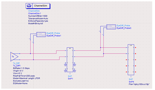
Do we have IBIS model for SN65DPHY440SS? My customer is evaluating SN65DPHY440SS and they want to simulate this part in ADS.

Can you kindly provide this model?

Another question, can we convert S-parameter model to IBIS model?

Tks and BRs

Marsh

  • Marsh

    We only have the s-parameter model(https://www.ti.com/product/SN65DPHY440SS#design-development) and encrypted HSPICE model available for DPHY440. Please let me know if you need the encrypted HSPICE model and I can send it to you in a private message. 

    I am not aware of a way to convert s-parameter model to IBIS model since the S-parameter model does not consider the specific form of the interconnection structure, and regards the interconnection structure simply as a black box.

    Thanks

    David

  • can we use these two model (s-parameter & HSPICE) to simulate in ADS software?

  • Hi,

    Both models are supported by the ADS software.

    For the s-parameter, it is a mix-mode s-parameter includes both differential mode (port 1-5) and common mode (port 6-10).

    For using encrypted HSPICE mode, please see this Keysight link, https://edadocs.software.keysight.com/display/ads2009/Encrypted+HSPICE.

    Thanks

    David 

  • Hi David.

    Do we have the appnote to introduce how to simulate S-parameter model inADS software?

    Customer now has some problem about this.

    tks & BRs

    Marsh

  • Marsh

    We don't have a user guide. 

    But the port order is 

    • Port 1 to Port 5 are differential ports for DA0 to DA3, e.g, S11 is the diff R/L for DA0P/DA0N, S22 is the diff R/L for DA1P/DA1N, ….
    • Port 6 to Port 10 are CM ports for DA0 to DA3, e.g, S66 is the CM R/L for DA0P/DA0N, S77 is the CM R/L for DA1P/DA1N, ….

    Below is an example of the ADS simulation setup.

    Thanks

    David

  • Hi David,

    Why TX and RX are separated into two files? How they interact with each other. I don't understand how to simulate the whole signal chain lane.

    It seems that the simulation for input signal is terminated at RX file. And it has no relationship with the TX file. In my understanding, S parameter is a  bidirectional parameter model show the relationship of INPUT and OUTPUT.

    Can the HSpice model you mentioned above used to simulate the relationship of INPUT and OUTPUT.

    Marsh

  • Marsh

    Why TX and RX are separated into two files? How they interact with each other. I don't understand how to simulate the whole signal chain lane.

    It seems that the simulation for input signal is terminated at RX file. And it has no relationship with the TX file. In my understanding, S parameter is a  bidirectional parameter model show the relationship of INPUT and OUTPUT.

    *** You have to simulate the TX and RX model separately. These models are s-parameter model and do not provide a full path from input to output.

    Can the HSpice model you mentioned above used to simulate the relationship of INPUT and OUTPUT.

    *** They should run two separate simulations, one for the RX, and another one for the TX. The model itself does not combine the RX and the TX.

    The model is a single lane model for High Speed mode only


    DPHY440_HS_RX_EQ_enc.hsp   //HSPICE file for single lane HS Rx


         //Pin List:


         //  vcc_1p8    Supply. Nominal 1.8V


         //  gnd        Ground


         //  d          Digitalized EQ output


         //  eqoutp     Positive EQ output


         //  da_p       Positive data input (DAxP pin of DPHY440)


         //  da_n       Negative data input (DAxN pin of DPHY440)


         //  eqoutn     Negative EQ output


         //  dz         Digitalized EQ output (reversed polarity)


         //  eq         Tri-level input for EQ level selection.


         //             0:0dB; 0.5*vcc_1p8:2.5dB; vcc_1p8:4dB


    DPHY440_HS_TX_enc.hsp  //HSPICE file for single lane HS TX


         //Pin List:


         //  erc_1      {erc_1,ecr_0} are 2-bits control for HS edge rate.


         //  erc_0      Logic High: 1.2V, Logic Low: 0V.


         //  data_in    HS-TX data input (from digital core), input high is 1.2V, input low is 0V.


                        Max 1Gbps.


         //  vsadj_1    {vsadj_1,vsadj_0} are 2-bits control for VOD.


         //  vsadj_0    Logic High: 1.2V, Logic Low: 0V.


                        00: 180mV  01:200mV (default)  1x: 220mV


         //  gnd        Ground


         //  vcc_1p8    Supply. Nominal 1.8v


         //  dout1p     Positive output. (DBxP pin of DPHY440)


         //  dout1n     Negative output. (DBxN pin of DPHY440)


    example file for tx and rx


    input_rx.hsp           //Reference simulation input file, trace/cable not included


    input_tx.hsp           //Reference simulation input file, trace/cable not included

    You would also need a HSPICE license to run the simulation.

    Thanks

    David