This thread has been locked.

If you have a related question, please click the "Ask a related question" button in the top right corner. The newly created question will be automatically linked to this question.

DP83822I: Pin 1 problem and Schematic Design Review Checklist Request

Part Number: DP83822I


Hi team

this is Joe, hope you have a nice day.

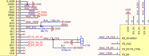
My customer uses DP83822 connect ESP32_WROVER_B to build the Wi-Fi block, PHY works in RMII Master mode.

Pin 1 of DP83822 is connected to ESP32_WROVER_B Pin IO0.

When write data to ESP32_WROVER_B, Pin IO0 need to be pulled to GND.

But after the data wrote into ESP32_WROVER_B, IO0 is always pulled to GND, and the Wi-Fi block cannot work properly.

Customer doubt that DP83822 PIn1 always pulls IO0 to GND.

Could you please check this problem, additionally, could you post the DP83822 design review check list, so that I can solve some problem independently.

Thank you!

  • Hi Joe,

    Is the device strapped correctly? Can you kindly review and provide a schematic? Attached is a template for reviewing your schematic, if you could fill it out I can review it when you're done.

    How does pin 1 (RX_D3) look like when RMII communication? (Should see 50 MHz Square wave)

    Regards,

    Alvaro

  • Hi Alvaro

    The picture is the DP83822 connection, MCU is on the left and DP83822 is on the right.

    You can see that in this circuit DP83822 pin1 is connected to MCU pin25(IO0), during the data download, MCU pin25 is pulled to GND using J1. when MCU need to work normally,J1 is disconnected and pin25 is pulled up through R17 by VDDIO(3.3V).

    But sometimes after J1 is disconnect, MCU pin25 cannot pulled up by VDDIO, customer doubt is that DP83822 pin1 always pull MCU pin25 to GND. in this condition, the internal resistance of DP83822 pin1 is 1k Ohm measured on PCB, but in normal condition it should be 10k Ohm.

    The above is the failure condition. If needed I can share the circuit file to you through e-mail.

    Thank you!

  • Hi Joe

    RX_D3 Pin 1 is an output pin driven strongly by the phy's internal 50 ohm driver. It should not be forced by MCU to ground. Only in the RESET State is this pin connected to 10 kOhms PD.  

    Regards,

    Alvaro