This thread has been locked.

If you have a related question, please click the "Ask a related question" button in the top right corner. The newly created question will be automatically linked to this question.

DS26F31MQML-SP: High Current Consumption whilst Enable' pin is held High

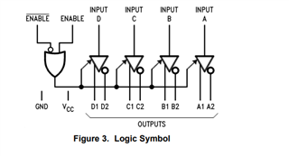
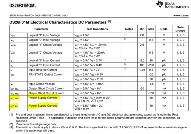
Part Number: DS26F31MQML-SP

Hello,

We have seen high current consumption(approximately 30 mA) while Enable'(active low) pin is held High and Enable(active high) pin is held as high. But when Enable' is held low (While Enable pin is still held as High),  the current consumption reduces to 19 mA. Could you please explain why current consumption is getting higher in that case?

Pin State Current Consumption(@VCC)

Enable
0 19 mA
Enable 1
Pin State Current Consumption(@VCC)

Enable
1 30 mA
Enable 1


Regards,

 Zafer Çalışkan

  • Zafer,

    Can you take a picture of the topside of the IC? Both of these currents seem high for ICC, so I want to make sure we're looking at the right device. Also, what else is happening with the device during the current measurement?

    Regards,

    Eric Hackett

  • Hi Eric,

    Sorry for my late reply. The actual part number written on the component is DS26F31MW/883. As written in my first post, when IC enable pins are set to "disable" case, the current drawn from the supply pin is increasing . Measurements are taken while there is no receiver IC is connected. So output pins are open circuit. 

    BTW, is it possible to mitigate SEU effects by disabling the output pins?

    Regards,

    Zafer Çalışkan

  • Additionally, is there any truth table that shows the output states versus enable pins?

  • Hi Zafer, 

    We've assigned the subject matter expert on this device to the thread, you should see a response in 24 hours.

  • Hi Zafer,

    Could you possibly send a picture of the top part of the part -I believe there should be more markings besides the part number itself.

    Also for truth table - there isn't an explicit one - however it can found in the datasheet from the functional block diagram or logic symbol:

    /ENABLE and ENABLE are OR'd together - so the truth table would look like this:

    ENABLE /ENABLE OUTPUT_STATE
    1 x Enabled
    x 0 Enabled
    0 1 Disabled (Hi-Z)

    Please let me know on the other markings from the part so I can see if I can trace the part number to check if its valid.

    Best,

    Parker Dodson

  • Hi Parker,

    Please see below picture for the part number. BTW, if we put the device in disabled case, is it possible to mitigate SEU effect such as stuck @1 or stuck @0 on output pins?

    Regards,

    Zafer Çalışkan

  • Thank You Zafer,

    The part number and markings look okay - so that's good.

    The disabled current is higher than the enable current on the device:

    This is due to the logic circuits shunting more current in the disable state compared to enabled state. It isn't super common in devices - but for this device that's how the datasheet states it will work. Minimizing current is to place 0V or VCC only on these enable pins (the closer to threshold the more current is shunted for ICC) as this test is using threshold values which will cause larger currents.

    What pin are you talking about on for the SEU to occur on? If an SEU even happens on one of the DI pins and the drivers are disabled it won't be transmitted on the bus - if you are speaking of something else please let me know!

    If you have any other questions please don't hesitate to reach out!

    Best,

    Parker Dodson

  • Hi Parker,

    Thank you for your reply.

    "What pin are you talking about on for the SEU to occur on? If an SEU even happens on one of the DI pins and the drivers are disabled it won't be transmitted on the bus - if you are speaking of something else please let me know!"

    Yes, we would like to know something like this. Actually, since there is no radiation report  for this IC, we don't know the failure characteristics on the pins when SEU happens. It would be so great if you can share a radiation test report for this IC. For now, it seems like we can only talk about the possibilities for failure modes of IC under radiation. For example, if DI or DO pin is stuck @1 or stuck @0, can we eliminate this by disable-enable cycle of output pins? Or do we need power cycling to eliminate persistent failures( stuck@1 or stuck@0  failures) on DI and DO pins? 

    Regards,

    Zafer Çalışkan

  • Hi Zafer,

    There is a radiation report - on the product page:

    https://www.ti.com/seclit/rr/snaa164/snaa164.pdf?ts=1663345187852&ref_url=https%253A%252F%252Fwww.ti.com%252Fproduct%252FDS26F31MQML-SP

    This is the radiation report we have provided for this part.

    For The SEU - I don't think this device is that sensitive to SEU's as it has no memory or registers - the state of the device is the state that is actively being input.

    If you are referring to a latch up event as that would closer fit the the fail scenario  - then it needs to be power cycled 

    Best,

    Parker Dodson

  • Hi Parker,

    Thank you for your reply.

    "For The SEU - I don't think this device is that sensitive to SEU's as it has no memory or registers - the state of the device is the state that is actively being input."

    There is no memory/register on IC but what about logic gates inside the transmitter? Are they like a combinational logic? If so, only SET can occur, Right?

    "If you are referring to a latch up event as that would closer fit the the fail scenario  - then it needs to be power cycled "

    Is there any possibility that  a latch-up can occur on DS26F31MQMML-SP? Becasue there is no information about that in IC's datasheet. If this is really possible, we need to take some precautions such as putting an LCL circuit to ICs supply pin. So could you please give a little bit more information about that?

    Regards,

    Zafer Çalışkan

  • Hi Zafer,

    For your first question - yes you are correct there is some level of combinational logic. However there is nothing saving state - from my understanding SEU's cause issues by changing a single bit causing a change of state in sequential logic circuits (so registers/memory as they have latches and flip-flops and they can save state without having to be constantly driven) and since the state is actively driven there isn't a save state to change. That being said - I do think a SET is possible on this pin. 

    So in general - if a device does not explicitly state that it is latch up immune - it probably isn't. Both Bi-polar and CMOS processes (anything with both P and N type devices without insulating trenches between the well/substrate or the use of guard rings) can lead to latching up and it requires a pretty concerted design effort to prevent it . A parasitic structure (thyristor)  can form a low impedance path between VCC and GND generally when one of the following conditions is met: 

    1. Pin voltage rises above VCC voltage turning on the parasitic structure.

    2. An Injected current above rating goes into a pin other than GND/VCC

    3. ESD Events (not super likely to cause latch up - but can; it depends how quickly the charge carriers dissipate after event) 

    4. Large transients at VCC pin - It would be best to keep this voltage under max ratings during transients.

    5. Applying larger than rec. voltage supply. 

    6. Ionizing radiation can trigger Latch up events (shouldn't latch up when used in accordance with provided radiation limits on device) 

    The first five items usually can be accounted for in the actual design process because it basically boils down to - don't exceed ratings. The 6th item shouldn't be much of an issue if the radiation limits are respected. The report I provided on the last response shows the change in key specs with different radiation levels applied. 

    Please let me know if you have any more questions!

    Best,

    Parker Dodson

  • Hi Parker,

    Once we checked the link below, it is stated that DS26F31 is bipolar. If this information is correct, since bipolar components are SEL immune, we are at the safe side in terms of Latch-up. But as looking at your comments, SEL seems to be related with TID level that the device is exposed(If my understanding is correct?). Generally for Single Event Effects(SEE), we need to check cross section diagrams for a given LET levels. But there is no radiation report for SEE. Could you please give us information about that?

    Link1: https://e2e.ti.com/support/interface-group/interface/f/interface-forum/1017263/ds26f31mqml-sp-see-seu-set/3765027?tisearch=e2e-sitesearch&keymatch=DS26F31#3765027

    Regards,

    Zafer Çalışkan

  • Hi Zafer,

    1. It is bi-polar - but it contains both PNP and NPN devices - if any PNPN junction forms - then latch up is possible; its more common in CMOS than bi-polar technology - but its not impossible. The thread you linked references an IEEE paper that tested a very similar device the paper doesn't say SEL is impossible - it just states that in the boundaries of the test it won't latch up - there is no cross section shown however so that determinization can't be made if there is a possibility for a parasitic PNPN junction to form - under tested limits this shouldn't be a concern which I alluded to in my last post. Also if you google "AE council bi-polar latch-up" you should find a detailed paper on how bipolar technology can cause latch-up. I can't share what we don't have public (so substrate design, and circuit internals) but under tested conditions it should be fine and SEL isn't a concern.

    2. SEL can have multiple root causes - including radiation. On the thread you linked the IEEE paper referenced has data about SEL - this device uses a very similar architecture so under rated conditions this shouldn't be a concern. 

    3. The closest radiation report is the IEEE paper referenced in that thread - as they tested a similar device for SEE. The specific reports on this part are provided on product page and that is the information that is available.

    Best,

    Parker Dodson