This thread has been locked.

If you have a related question, please click the "Ask a related question" button in the top right corner. The newly created question will be automatically linked to this question.

SN65LVDT2: SN65LVDT2DBVR

Part Number: SN65LVDT2
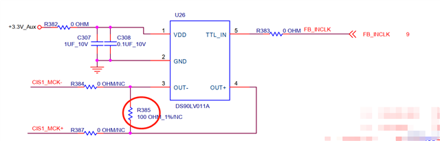
Other Parts Discussed in Thread: DS90LV011A

Hello TI experts:

the above is SN65LVDT2 waveform, TP4 is Output PIN,which alway keep Low level, normally TP4 should be output normal clock;

the transmiter IC is DS90LV011A from controller board,after add 1K ohm resistor near to DS90LV011A chip, we can get normal output from SN65LVDT2 as below.


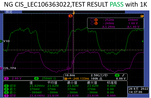
Can someone take a look tell me what is different between two waveform picture, i do not know which parameter on NG CIS can not meet SN65LVDT2 spec. 

  • Hi Toms,

    after add 1K ohm resistor near to DS90LV011A chip, we can get normal output from SN65LVDT2

    Could you help clarify what the resistor is connected to; while helping to share the schematics? Thanks.

    Best Regards,

    Michael.

  • Hi Michael

    Thanks for you quickly replied.

    Original we mounted R384&R387 with 0 OHM, Considering SN65LVDT2 have internal terminal resistor(110 OHM),so we did not R385 is non-pop.

    but if R385 non-pop, LVDS receiver chip(SN65LVDT2)will be no output;after we put 1K with R385, we can get output waveform;  

  • Hi Toms

    SN65LVDT2 has integrated internal impedance  but it can only be used in a point-to-point system or in a multi-drop system when it is the last receiver on the multidrop bus. Otherwise the change of bus impedance throughout the bus will result in multiple reflections and signal distortion.

    It's hard to tell the application is correct with partial schematic. Please share the complete schematic with receiver (SN65LVDT2) included so we can help you better.

    Thanks,

    Yuan

  • please refer the application schematic, we also tried to remove C65&C66 on CIS board, but the issue still exists.

  • Hi Toms,

    You are right, SN65LVDT2DBV has an internal 110-Ohm termination. Hence, no termination needed for the receiver.

    However, the driver would also need it's termination as well; as we recommend to match that of the receiver to further help avoid impedance mismatch for transmission line effects, thanks.

    Best Regards,

    Michael.

  • HI Michael

    Thank you, it means that we mounted R385 with 1K ohm shoud be reasonable for impedance mismatch.

    Can you share me which parameter is out of SN65LVDT2DBV spec. based on above waveform? we wanna to know if R385=1K ohm is suitable for this application.

    pls:we also tried other values with R385,such as 100ohm/390ohm, but some of product can not work well,some of product can works well.

    Thanks

    Toms

  • Hi Toms,

    A lot of factors could impact transmission line effects (See High Speed Layout Guidelines).

    For the impedance mismatch, you would have to match that of the cabling as well. Hence, if the cable's differential pairs are 50 ohms each, a 100 ohm termination should work well similar to section 1.3.2 discussed, thanks.

    Best Regards,

    Michael.

  • Is it possible to check waveform and point out which one(rising time/fall time/holding time..etc) did not meet the part spec? we can know what is good design by signal check.thank you.

  • Hi Toms,

    Could you help double confirm the impedance of the cabling? Thanks.

    Best Regards,

    Michael.

  • HI Michael,

    we use normal FFC cable, did not do impedance control for this cable.

    Do you say this cable should have impedance control for Clock signal?

  • Hi Toms,

    The waveform seems to show transmission line effects for the reflections observed (High Speed Layout Guidelines) and would suggest matching the impedance, so as to help mitigate the observed reflections, thanks.

    Best Regards,

    Michael.

  • LVDS Unlock Issue FA Report-To TI_20221026.pdf

    Hi Michael

    We tried change LVDS input voltage from 200mV to 500mV, the product function is OK, but we have three questions as below:

    1.what is Input signal critical for normal output,--check the waveform, we can see the output with VIN=350mV, some of IT parts can have normal output waveform, but some of IC no output,why? 

    2.why the output with 200mV/350mV input signal is normal pulse, but 500mv input signal is spike pulse output?

    3.what is Eye pattern spec. for this part input signal?

  • Hello Toms,

    To answer question 1 and 2, could you help us better understand what are the changes in each case 1-4?

    3) For eye diagram patterns, input is usually generated by a Bit Error Rate Tester (BERT) that generates a PRBS pattern (typically 2^31 -1). The typical test conditions used below:

    Input Differential Voltage = 200 mVpp

    Vcm = 1V

    tr=tf=0.5 ns (10% to 90%) 

  • Case1~4 means when we tested 13PCS CISM(CMOS Image Sensor Module),

    some of CISM waveform shows as case 1(Vout=0 no output with Vin=200mV , Vout=0 no output with Vin=350mV,Vout=Spike pulse with Vin=500mV) ;

    Some of CISM waveform shows as case 2 (Vout=0 no output with Vin=200mV , Vout=Spike pulse with Vin=350mV,Vout=Spike pulse with Vin=500mV) ;

    Some of CISM waveform shows as case 3 (Vout=normal pulse with Vin=200mV , Vout=normal pulse with Vin=350mV,Vout=Spike pulse with Vin=500mV) ;

    the output waveform as case4 is what we want; 

  • Hello Toms,

    Did you use different types of CMOS Image Sensor Modules? Was there one FFC cable used for all cases or were multiple cables used? If everything in the circuit is exactly the same, then you will see the same output (similar to the 500mV input signal in case 1-3). 

    Is it possible to take some measurements? Referring to the Application Schematic you posted, could you compare the differential voltage coming out of the DS90LV011A (R384 and R387) and the differential voltage coming into the SN65LVDT2 (R41 and R42)? It's possible the FFC cable could be the root cause.

  • Sorry to make you confused, for LVDS schematic,please kindly refer the attached updated file,We used same one FFC cable+Same one Controller board with Option1(LVDS drive from SOC_U15) to test 13PCS CMOS Image sensor Modules; 13PCS CISM type is same, only serial number is different; but SN65LVDT2DBV output waveform on each CISM(CMOS Image Sensor Modules)is quite different as FA report shows. So I have two questions as below:

    1.what is Input signal critical for normal output,--check the waveform, we can see the output with VIN=350mV, some of IT parts can have normal output waveform, but some of IC no output,why? 

    2.why the output with 200mV/350mV input signal is normal pulse, but 500mv input signal is spike pulse output like case3?

     LVDS HW Structure-To TI_1028.pdf

    Remark for hardware:the history is firstlly we use 200mV drive from SOC,we found some of CISM can not get normal output from SN65LVDT2DBV, so we tried to change to Option2,drive from external LVDS driver IC, but still have few CISM failed on no output;

    So we changed back to option1 with 500mV drive from SOC, all of CISM have output waveform, but some of output is spike pulse,some if output waveform is normal pulse; we do not why this difference happen?how to judge the input signal quality is acceptable by SN65LVDT2DBV to generate normal output?

  • Hello Toms,

    Appreciate the clarification.

    1) For the DS90LV011A, if meeting the device's V(IL) and V(IH) levels, then there shouldn't be an issue with the output. Meaning there isn't a critical input signal that gives a normal output. As long as the device's specs are met, the device will give the typical output. That being said, it's also recommended to have the input be symmetrical to the voltage threshold of the driver. This will minimize any skews in the LVDS system. More information can be found here: Keep An Eye On The LVDS Input Levels.

    On the SN65LVDT2, the input differential voltage should be above +100mV and below -100mV (based on the truth table found on Section 9.4.5 on the datasheet) but the input differential voltage cannot be greater than 1 V. This goes above the absolute max spec for the receiver.

    2) Can you replicate Case 2 and Case 3 with the 200mV input and capture the signal at R384 & R387 (CTL Board) and R41 & R42(CISM Board)? Additional measurements you need to be taken before we can find a proper solution.

    Regards,

    Josh

  • 2) Can you replicate Case 2 and Case 3 with the 200mV input and capture the signal at R384 & R387 (CTL Board) and R41 & R42(CISM Board)? 

    ---case1~case4, we tested waveform based on LVDS signal drive from U15,not external LVDS driver IC U26.

    Do you say we need to capcture waveform at R372&R373 for case2 and case3 with 200mV?

  • Help Toms,

    My apologies, I initially thought the waveforms you shared were captured using the external LVDS driver. In that case, yes if you can replicate case 2 and case 3 with 200mV input and share the waveform at R372 & R373 and R41 &R42 that would be helpful. 

    Regards,

    Josh

  • Please kindly check the waveform as the attached fileLVDS Unlock Issue FA Report-waveform compare_1101.pdf

  • Hello Jusua

    If you need to have more test for you view, please let me know.

  • Hello Toms,

    Thanks for the waveform captures. I will take a look at them and respond later today.

    Regards,

    Josh

  • Hello Toms,

    Thanks for your patience.

    At the bottom of the waveforms capture, can you help me translate the wording? We have to make sure the input differential voltage going into the SN65LVDT2 is higher than +100mV and lower than -100mV. Figure 12 on the datasheet gives an example.

    And just to double check, in both CISM boards is every component populated that same way? For instance C65 is populated on one board but not the other.

  • And just to double check, in both CISM boards is every component populated that same way?--Yes

    For instance C65 is populated on one board but not the other.--No, C65&C66 is populated on everyLVDS Unlock Issue FA Report-To TI_1103.pdf CISM board.

  • Toms,

    Is it possible to remove the SN65xx device on Case 3 and place it on Case 2 and try the measurements again?

    Regards,

    Josh

  • LVDS Unlock Issue FA Report-20221114.pdf

    Hello Josh

    Thanks for your comments.

    Finally we found the cause is R41 resistance various from 47 ohm~2K ohm, some of R41 resistor value even open.

    visual check we found R41 is damaged, checked with Vendor R41 is damaged by production jig.

    Again, Thank you all.