


Part Number: DP83826E
Hello,
I'm working on a board and we're trying to design in the DP83826. I generally understand the concept of bootstrap pins to allow for quick config/behavior after power on reset.
In general, I see many pins either have an internal pull-up or pull-down resistors assigned to them.

Also, each of the bootstrap specific pins have default values assigned to them.
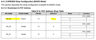
I want to make sure I understand the relationship between the default values and the specified PU/PD assignments per pin. In the example above, in basic mode, the table indicates the DEFAULT value of RX_D3/PHY_ADD0 is 1. To me, this would indicate an internal pull up is present on that pin.
However, when I look at table 7-1 of the data sheet, the table indicates RX_D3 is assigned a pull-down on power up. This indicates to me that the 'default' value of that pin would be 0, not 1 as indicated in table 9-14.
In addition, I'd like to clarify, that in section 9.4.1.2, that if a DEFAULT state listed matches my desired chip config, I do not need to add any external pull up or pull down resistors. For example, Table 9-16 indicates the default behavior is that Auto Negotiation is enabled, therefore, I don't need to have any external pull-ups / pull-downs added?
However, as another example, I want my design to come out of reset with full-duplex enabled, therefore I need to add a 2.49k pull down to pin16 (LED1/TX_ER) to get the mode to register as 0 (full duplex) on power up.
Thank you for any clarification you can provide on this.
