This thread has been locked.

If you have a related question, please click the "Ask a related question" button in the top right corner. The newly created question will be automatically linked to this question.

TCAN4550: read/write config registers

Part Number: TCAN4550

Customer is currently working on TCAN4550 device which is connected to microcontroller through SPI(Serial peripheral Interface ) with 5MHz clock speed and Mode 0 ( CPOL=0  CPHA=0 ).

With the above SPI configuration I am able to read  Device ID and Interrupt/Diagnostic Flag Registers( 16'h0000 to 16'h002F) but I am not able to read/write Device Configuration Registers( 16'h0800 to 16'h08FF) , Interrupt/Diagnostic Flag and Enable Flag Registers( 16'h0820/0824 and 16'h0830) and  CAN FD Register Set (16'h1000 to 16'h10FF).

Could you please let me know what could be the possible issue which is not allowing me to read/write registers other then 0x0000 to 0x002F.

  • Hi Prahlad,

    This sounds like there is an issue with your device clock connected to the OSC1/2 pins. I don't know if this is configured for a crystal or a single-ended clock interface, but it needs to have a 20MHz or 40MHz clock running in order to access registers outside of the 0x0000 to 0x002F space. 

    The 0x0000 to 0x002F register space is implemented such that it does not need the digital core to be functional to communicate through SPI.  However, every other register or MRAM (Memory RAM) address in the device requires the digital core to be operational, and therefore it needs a functional clock to drive the digital core.  

    To handle the SPI clock to digital core clock frequency transition, a FIFO is used and it requires the digital core clock be at least 2MHz faster than the SPI clock frequency.  This is evident by the maximum SPI clock frequency of 18MHz with minimum oscillator clock of 20MHz.

    However, if this oscillator clock is missing, or too close to the SPI clock frequency, the device will not be able to access the internal register or MRAM space and return the data causing the SPI read/write transactions to fail.

    You should also check the reset pin (RST) is LOW because this is an Active High reset pin which is less common than an Active Low.  If this pin is connected to the MCU, or has a pullup resistor instead of a pulldown resistor, and the RST pin is HIGH, the device could be held in a reset condition.

    Also check the voltage levels of the VSUP, VIO, and VCCOUT pins have the correct voltage levels.

    Regards,

    Jonathan

  • Verified that Crystal is running at 40Mhz,Reset pin is in LOW state, VSUP, VIO, and VCCOUT pins are as expected but still not able to read  registers outside of the 0x0000 to 0x002F space. Could you please suggest any alternative 

  • Hi Basaveshwar,

    Can you tell me what value you are reading for the Status register (0x000C)?  Are any bits getting set?

    Can you share any scope or logic analyzer plots of the SPI signals for both the registers you are able to successfully read, and also the ones you are not able to read (i.e. 0x0800+)?

    Are you using a TCAN4550 device on a board you have developed, or on a purchased board from TI such as the TCAN4550EVM or BOOSTXL-CANFD-LIN?  If it is a board you have developed, could you share the portion of the schematic for the TCAN4550  configuration so that I can check it as well?

    Regards,

    Jonathan

  • Hi Jonathan,

    On replacing the crystal , now TCAN4550 is working as expected. Thanks for your support.

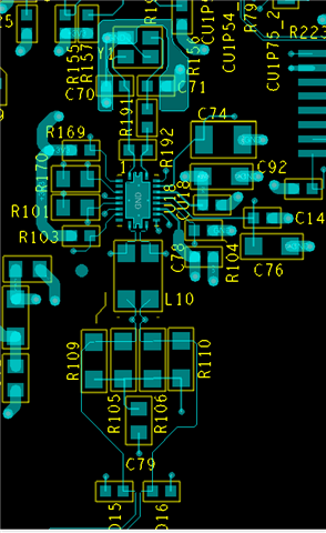
    I have quarry on Layout.  Please find the attached layout options that we are evaluating.  Can you please conform which may hold the best placement?

    Few important Highlights:-

    1. R105, 109 are 120 ohm in parallel (hence 60 ohm effectively) to improve the power of the resistors.
    2. R106, 110 are 120 ohm in parallel (hence 60 ohm effectively) to improve the power of the resistors.
    3. In Options1 it not possible to route the signal in 120 Ohm differential From L10 to connector as they are signal net and passing through the components.  Hence trace width and separation has to managed manually (Routing like differential).
    4. In Options2 it will be possible to maintain 120 Ohm differential routing.
    5. D15 and D16 will be moved near connectors.

     Please confirm on the same.(we tested and made working with Option 1)

    Option1

    Option2

  • Hi Basaveshwar,

    I think either option 1 or option 2 would work.  On our device evaluation boards we regularly split up the differential routing to single ended routing near the termination resistors, TVS diodes, and common mode choke.  When you do split the routing to single ended, you can change the trace width to a 60 ohm single-ended instead of the 120 ohm differential.  But realistically the impedance discontinuity of the component pads is still present.  Also, the total length of the discontinuities is very short compared to the entire CAN bus length, so either option should be fine.

    In looking at the crystal layout, I believe R191 should be moved to the OSC1 pin which is the Output of the Transimpedance Amplifier providing current to the crystal.  This series resistor is used to dampen the current flowing through the crystal and make sure the drive level (or power dissipation in the crystal) is not too large.  Also, the TCAN4550 has an internal 500k ohm feedback resistor between OSC1 and OSC2 pin so R192 is optional.

    You can find more information about optimizing the crystal in the TCAN455x Clock Optimization and Design application note.

    Regards,

    Jonathan